Simulation method for optical characteristics of cesium tin bromide-molybdenum disulfide composite material
A technology of molybdenum disulfide and optical properties, which is applied in the field of materials science, can solve the problems of insufficient optical properties and low carrier mobility of cesium tin bromine, and achieve improved carrier mobility, excellent environmental protection, and improved optical properties. The effect of the characteristic
- Summary
- Abstract
- Description
- Claims
- Application Information
AI Technical Summary
Problems solved by technology
Method used
Image
Examples
Embodiment 1
[0045] Comply with above-mentioned technical scheme, present embodiment provides a kind of CsSnBr 3 / MoS 2 Composite model and CsSnBr 3 A method for improving optical properties, the perovskite used is CsBr-CsSnBr 3 (100) surfaces. The specific steps are:
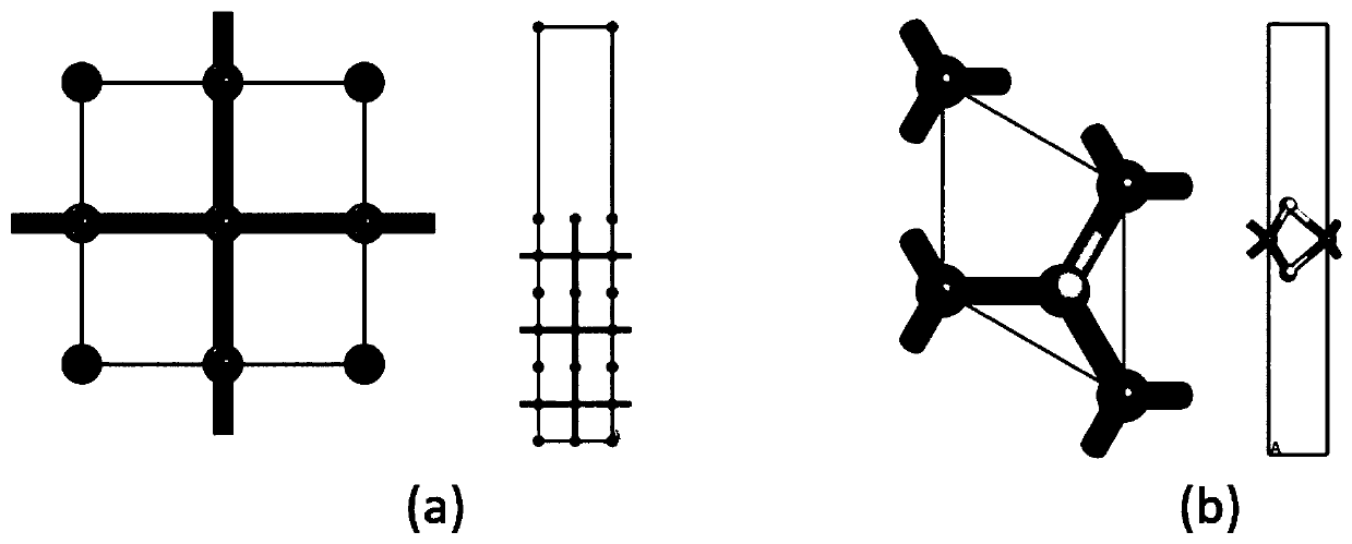
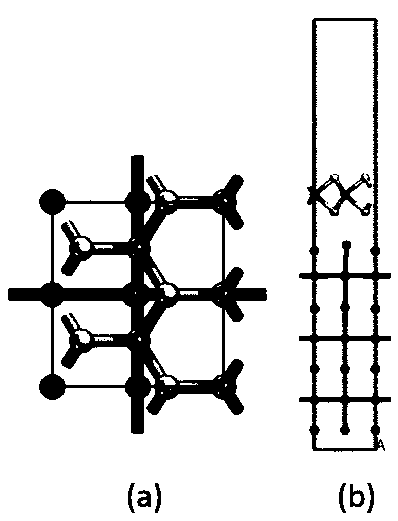
[0046] S1. In the Materials Studio 2017 software, respectively establish 7 layers of CsBr-CsSnBr 3 (100) surface and monolayer molybdenum disulfide (MoS 2 ) model, such as figure 1 As shown, simulated by the CASTEP module in the Materials Studio 2017 software package;
[0047] S2. To illustrate the van der Waals interaction between cesium tin bromide and molybdenum disulfide, a hybrid semi-empirical solution of OBS is applied in DFT-D to introduce damping atom pairwise dispersion correction.
[0048] The configuration of the valence atom is 4d for the Mo atom 5 5s 1 , the S atom is 3s 2 threesome 4 , Cs atom is 5s 2 5p 6 6p 1 , the Sn atom is 4d 10 5s 2 5p 2 , Br atom is 4s 2 4p 5 .
[0049] The cut-off ...
Embodiment 2
[0065] Comply with above-mentioned technical scheme, present embodiment provides a kind of CsSnBr 3 / MoS 2 Composite model and CsSnBr 3 A method for improving optical properties, the perovskite used is SnBr 2 -CsSnBr 3 (100) surfaces. The specific steps are:
[0066] Step S1 and step S2 are the same as in embodiment 1, except that the surfaces of the two cases are different.
[0067] The above results are analyzed as follows:
[0068] MoS 2 The energy band structure diagram is as Figure 5 As shown in (a), SnBr 2 -CsSnBr 3 (100) The surface energy band structure diagram is as follows Figure 5 As shown in (c), SnBr 2 / MoS 2 Composite model energy band structure diagram as shown in Figure 5 (e) shown. MoS 2 and SnBr 2 -CsSnBr 3 The surface of (100) shows a direct band gap, and after forming a heterojunction, the bottom of the conduction band is mainly composed of MoS 2 contribution, the valence band top is mainly composed of CsSnBr 3 contribution, and simila...
PUM
 Abstract
Description
Claims
Application Information


