

Method for manufacturing gate oxide layer on silicon carbide material
A technology of gate oxide layer and manufacturing method, which is applied in the direction of semiconductor/solid-state device manufacturing, electrical components, circuits, etc., can solve the problems of the number of trapped charges in the interface state and the reduction of oxide layer charges, and achieve the improvement of threshold voltage and channel good mobility
- Summary
- Abstract
- Description
- Claims
- Application Information
AI Technical Summary
Problems solved by technology
Method used
Image

Examples
Embodiment 1
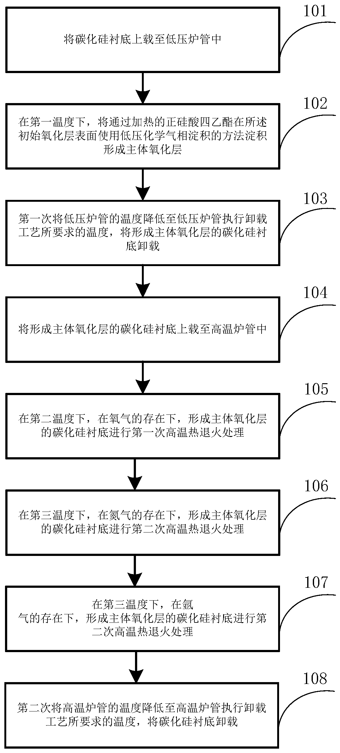
[0034] figure 1 It is a schematic flow chart of a method for manufacturing a gate oxide layer on a silicon carbide material provided in an embodiment of the present invention, as shown in figure 1 As shown, the present invention proposes a method for manufacturing a gate oxide layer on a silicon carbide material, comprising the following steps:
[0035] In step 101, a silicon carbide substrate is provided and placed in a low-pressure furnace tube;
[0036] Continue to set the pressure of the low-pressure furnace tube to 0.2mbar, raise the temperature inside the low-pressure furnace tube to 650°C at a rate of 5°C / min, and heat tetraethyl orthosilicate to 30°C;
[0037] In step 102, a body oxide layer with a thickness of 50 nm is deposited on the surface of tetraethyl orthosilicate silicon carbide substrate heated to 30° C. by means of low-pressure chemical vapor deposition;
[0038] In step 103, the temperature of the low-pressure furnace tube is lowered at a rate of 5°C / min ...
Embodiment 2
[0053] figure 1 It is a schematic flow chart of a method for manufacturing a gate oxide layer on a silicon carbide material provided in an embodiment of the present invention, as shown in figure 1 As shown, the present invention proposes a method for manufacturing a gate oxide layer on a silicon carbide material, comprising the following steps:
[0054] In step 101, a silicon carbide substrate is provided and placed in a low-pressure furnace tube;
[0055] Continue to set the pressure of the low-pressure furnace tube to 0.3mbar, raise the temperature inside the low-pressure furnace tube to 700°C at a rate of 10°C / min, and heat tetraethyl orthosilicate to 42°C;
[0056] In step 102, a body oxide layer with a thickness of 60 nm is deposited on the surface of tetraethyl orthosilicate silicon carbide substrate heated to 42° C. by low-pressure chemical vapor deposition;
[0057] In step 103, the temperature of the low-pressure furnace tube is lowered at a rate of 10° C. / min to 45...
Embodiment 3
[0067] figure 1 It is a schematic flow chart of a method for manufacturing a gate oxide layer on a silicon carbide material provided in an embodiment of the present invention, as shown in figure 1 As shown, the present invention proposes a method for manufacturing a gate oxide layer on a silicon carbide material, comprising the following steps:
[0068] In step 101, a silicon carbide substrate is provided and placed in a low-pressure furnace tube;
[0069] Continue to set the pressure of the low-pressure furnace tube to 0.5mbar, raise the temperature inside the low-pressure furnace tube to 750°C at a rate of 15°C / min, and heat tetraethyl orthosilicate to 50°C;
[0070] In step 102, a body oxide layer with a thickness of 70 nm is formed by depositing tetraethyl orthosilicate silicon carbide substrate surface heated to 50° C. by means of low-pressure chemical vapor deposition;
[0071] In step 103, the temperature of the low-pressure furnace tube is lowered at a rate of 15° C....
PUM
| Property | Measurement | Unit |
|---|---|---|
| Thickness | aaaaa | aaaaa |
| Thickness | aaaaa | aaaaa |
| Thickness | aaaaa | aaaaa |
Abstract
Description
Claims
Application Information