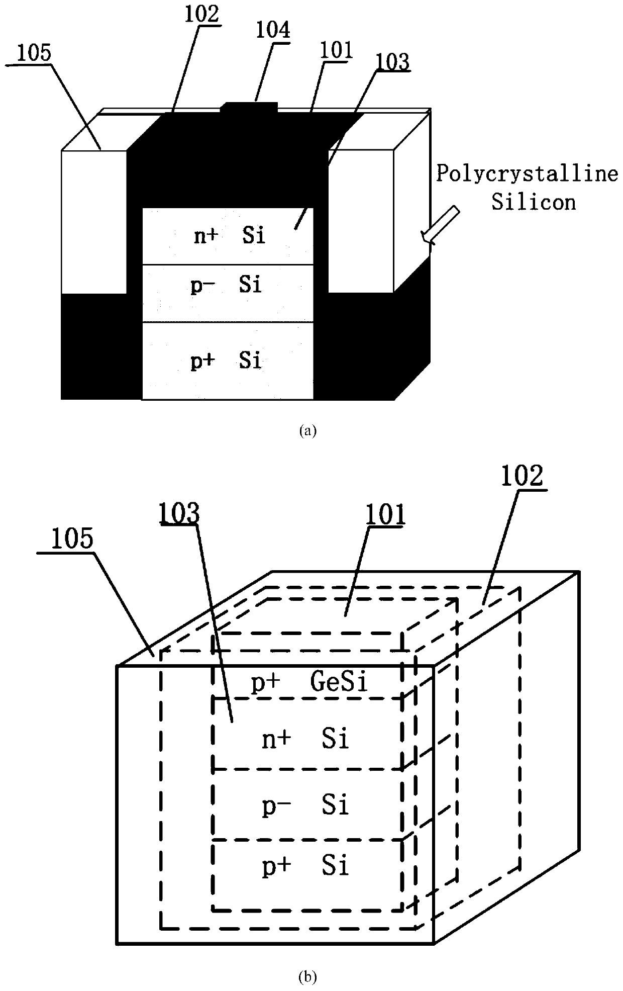
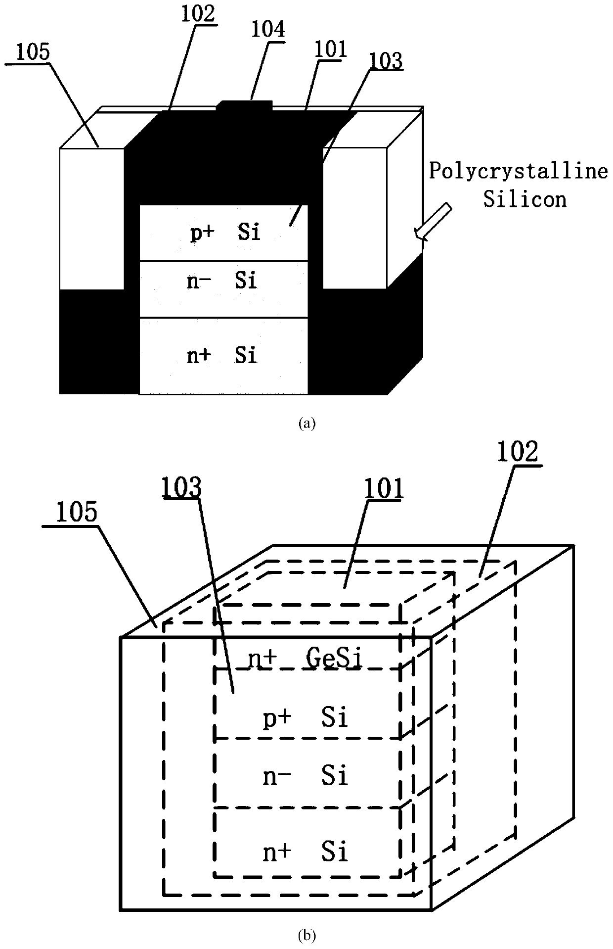
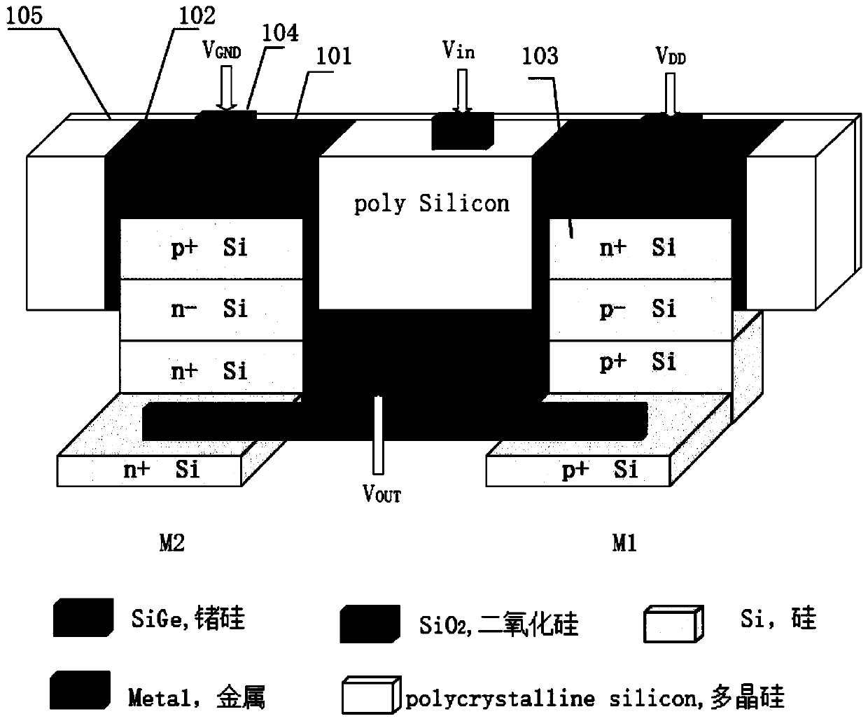
Structure of novel digital gate integrated circuit
An integrated circuit, a new type of technology, applied in the field of microelectronics technology and semiconductor technology, can solve problems such as complex processes, and achieve the effects of strong control ability, cost saving, and improved withstand voltage
- Summary
- Abstract
- Description
- Claims
- Application Information
AI Technical Summary
Problems solved by technology
Method used
Image

Examples
Embodiment 1
[0046] Embodiment 1: The realization process of NOT gate process of the present invention:
[0047] (a) silicon wafer preparation;
[0048] (b) growing a layer of sacrificial material (such as silicon nitride, etc.);
[0049] (c) epitaxially growing the drain, channel, and source of the PMOS transistor;
[0050] (d) stripping and growing sacrificial material again;
[0051] (e) Epitaxial growth of NMOS transistor drain, channel, and source;
[0052] (f) Coating and photolithography after stripping;
[0053] (g) using a photoresist as a mask to etch down the epitaxially grown doped SiGe layer and doped Si layer;
[0054] (h) Anisotropic growth of SiO 2 , and then grow a layer of polysilicon as the gate electrode, and wash off the photoresist;
[0055] (i) glue again, photolithography;
PUM
 Abstract
Description
Claims
Application Information