Check patentability & draft patents in minutes with Patsnap Eureka AI!

LDMOS device and process method

A process method and device technology, applied in the field of NLDMOS devices, can solve problems such as unsatisfactory breakdown voltage of LDMOS devices

Pending Publication Date: 2020-04-24
SHANGHAI HUAHONG GRACE SEMICON MFG CORP
View PDF0 Cites 2 Cited by
  • Summary
  • Abstract
  • Description
  • Claims
  • Application Information

AI Technical Summary

Problems solved by technology

[0005] The breakdown voltage BV or characteristic on-resistance of the LDMOS devices with the above two structures Neither is ideal

Method used


Image

  • LDMOS device and process method
  • LDMOS device and process method
  • LDMOS device and process method

Examples


Embodiment 1

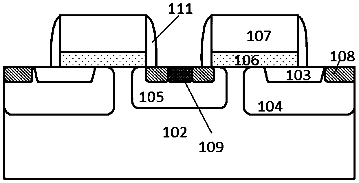
[0060] An LDMOS device according to the present invention, such as image 3 As shown, the P-type substrate 102 (or P-type epitaxy) has a P-type body region 105 and an N-type drift region 104 .

[0061] There is also a polysilicon gate structure on the surface of the P-type substrate, and the polysilicon gate structure includes a gate dielectric layer 106, a polysilicon gate 107, a metal silicide 110 above the polysilicon gate, and gate spacers 111, so The gate dielectric layer is located on the surface of the substrate to isolate the polysilicon gate from the substrate, and the spacers are located on both sides of the polysilicon gate.

[0062] The polysilicon gate structure is located on the surface of the substrate between the P-type body region and the N-type drift region, and overlaps with the body region 105 and the drift region 106 located on both sides thereof, that is, image 3 The middle polysilicon gate structure covers the body region 105 to the left and the isolat...

Embodiment 2

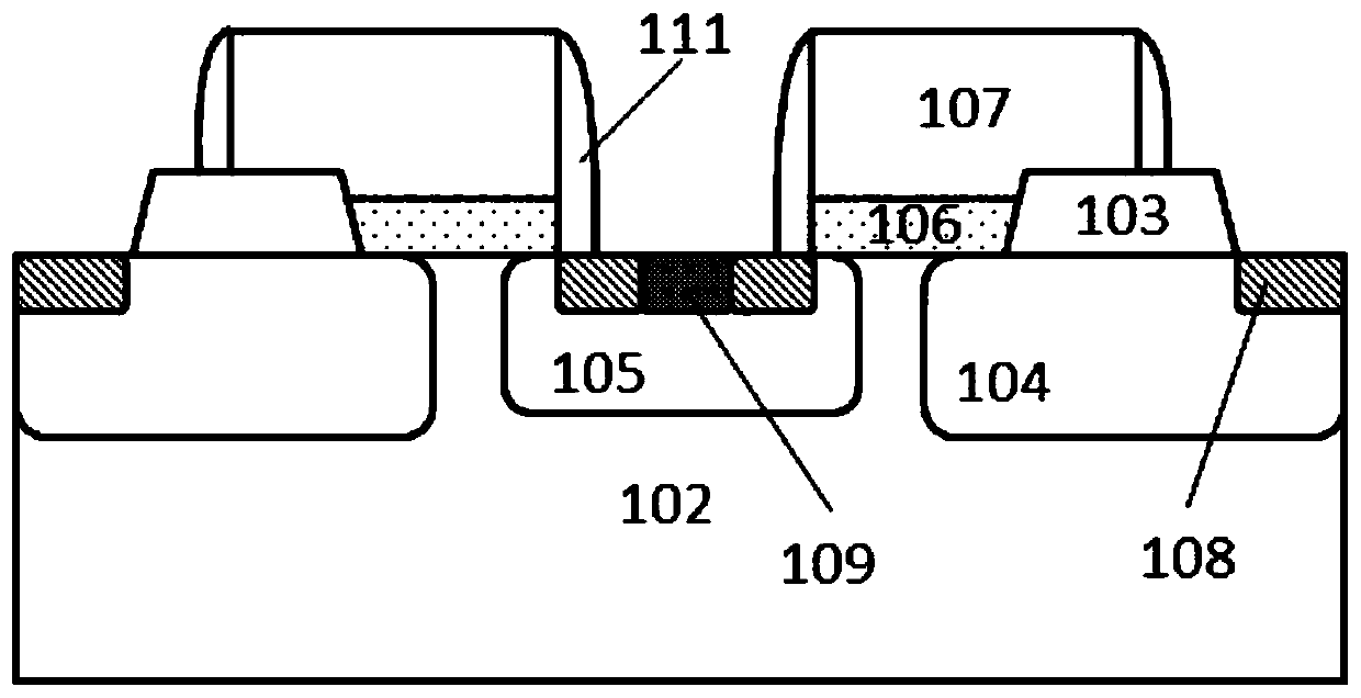
[0078] Another LDMOS device provided by the present invention, such as Figure 7 As shown, its main structure is roughly the same as that of the first embodiment, and will not be repeated. The difference from the first embodiment is that the isolation silicon oxide layer 103 is located on the surface of the substrate, and the structure of the first embodiment is An isolation silicon oxide layer 103 is embedded in the substrate.

[0079] One side of the isolation silicon oxide layer 103 extends below the polysilicon gate structure and is connected to the gate dielectric layer, that is, embedded in the polysilicon gate, and the other side is connected to the N-type dopant in the N-type drift region. The nearest side of the miscellaneous region 108 is aligned.

[0080] The isolation silicon oxide layer 103 also has a metal silicidation reaction blocking silicon oxide layer 101 .

[0081] The thickness of the isolation silicon oxide layer 103 is defined as the thickness of the f...


PUM


Abstract

The invention discloses an LDMOS device. A body region of a first conductivity type and a drift region of a second conductivity type are arranged in a substrate of the first conductivity type, and the body region of the first conductivity type further comprises heavily-doped doped regions of the first conductivity type and the second conductivity type. Metal silicide is arranged above the first conductive type doped region and the second conductive type doped region. The drift region of the second conductive type comprises a heavily-doped doped region of the second conductive type and metal silicide positioned above the doped region of the second conductive type. An isolation silicon oxide layer is arranged in the drift region of the second conduction type. One side of the isolation silicon oxide layer extends below a polycrystalline silicon gate structure, and the other side of the isolation silicon oxide layer extends to the second conductive type doped region in the second conductive type drift region. A metal silicification reaction blocking silicon oxide layer is further arranged above the isolation silicon oxide layer. According to the invention, a better BV-Rsp relation canbe obtained. The process method provided by the invention can be compatible with a BCD process.

Description

technical field [0001] The invention relates to the field of semiconductor integrated circuit manufacturing, in particular to an NLDMOS device. The present invention also relates to a process method of the NLDMOS device. Background technique [0002] DMOS (Double-diffused MOS) is currently widely used in power management chips due to its high voltage resistance, high current drive capability and extremely low power consumption. In LDMOS (Lateral Double-diffused MOSFET, Lateral Double Diffused Field Effect Transistor) devices, on-resistance is an important indicator. In BCD (Bipolar-CMOS-DMOS) process, although LDMOS and CMOS are integrated in the same chip, due to the contradiction between high breakdown voltage BV (Breakdown Voltage) and low characteristic on-resistance (Specific on-Resistance) / A compromise often fails to meet the requirements of switching tube applications. High-voltage LDMOS not only has the characteristics of high-voltage and high-current of discrete...

Claims


Application Information

Patent Timeline
IPC IPC(8): H01L29/78H01L29/40H01L29/06H01L21/336
CPCH01L29/7817H01L29/404H01L29/0615H01L29/0653H01L29/66681
Inventor 许昭昭
Owner SHANGHAI HUAHONG GRACE SEMICON MFG CORP
Features
  • R&D
  • Intellectual Property
  • Life Sciences
  • Materials
  • Tech Scout
  • Unparalleled Data Quality
  • Higher Quality Content
  • 60% Fewer Hallucinations
Learn More