Broadband CMOS second-order active balun amplifier

An amplifier and broadband technology, applied in the field of microelectronics, can solve problems such as gain error, phase error, and current signal phase error, and achieve the effects of compensating gain attenuation, small phase error, and small gain error

Active Publication Date: 2020-05-08
XIDIAN UNIV
View PDF9 Cites 5 Cited by
  • Summary
  • Abstract
  • Description
  • Claims
  • Application Information

AI Technical Summary

Problems solved by technology

Under the premise of avoiding the use of signal switches to introduce additional insertion loss and additional noise, the invention makes up for the shortcomings of the passive balun's excessive volume in the intermediate frequency band, and at the same time solves the problem that the traditional active balun circuit cannot realize the signal bidirectional conversion function.
However, the shortcomings of the intermediate frequency bidirectional active balun still exist in that the single-transistor dual-circuit part of the invention adopts the single-transistor separation structure active balun structure, and realizes the differential output through simple and practical operation, which is far lower It also has a very accurate differential phase when working in the low frequency band of the millimeter wave MMW (Millimeter Waves) frequency
However, the disadvantage of this broadband active balun circuit is that the high-frequency parasitic circuit of the active balun structure of the source follower and common-gate amplifier will cause additional signal delay or cause the signal to pass through different loads, so the current signal There will be a certain phase error when passing through the common gate amplifier, and it will not be completely inverted when passing through the amplifier
Additional parasitic effect compensation technology is required to compensate for the generated errors, making the circuit have larger power consumption and lower gain
Also, in the second-order differential amplifier P 8 and P 9 Due to the size and threshold voltage mismatch between transistors, the current and transconductance flowing through the two transistors are also different. Due to the mismatch between transistors, a certain phase error and gain error will also be generated.

Method used


Image

  • Broadband CMOS second-order active balun amplifier
  • Broadband CMOS second-order active balun amplifier
  • Broadband CMOS second-order active balun amplifier

Examples


Embodiment Construction

[0019] Below in conjunction with accompanying drawing, the present invention is further elaborated.

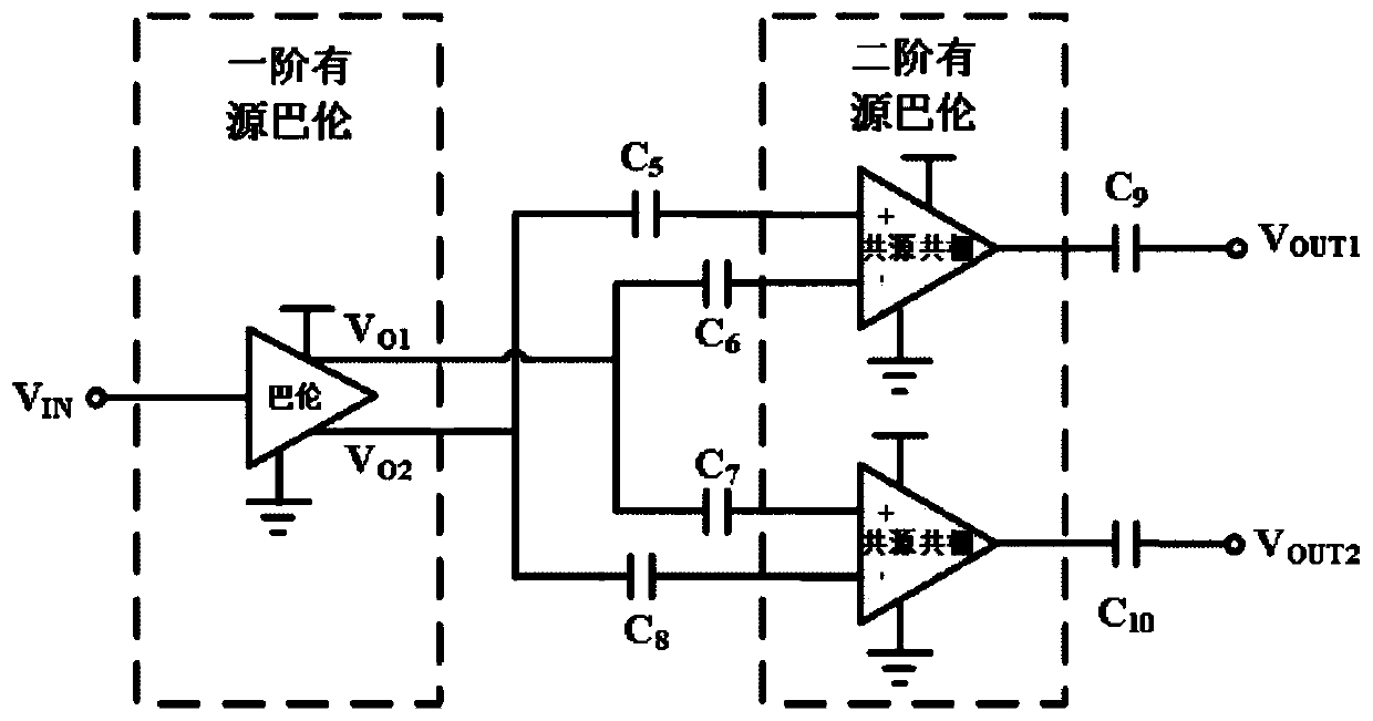
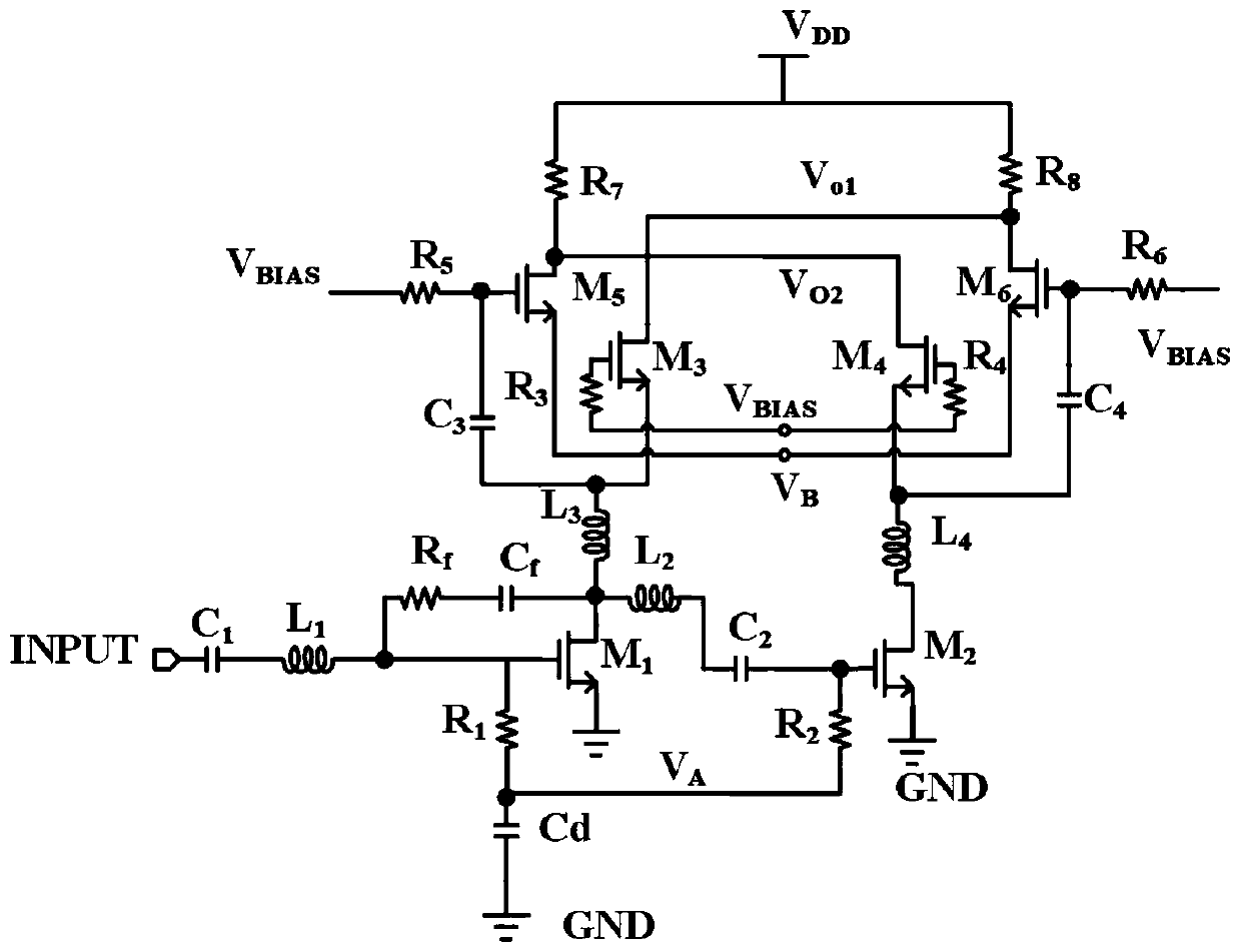
[0020] refer to figure 1 Further elaboration on the overall circuit structure topology of the present invention.

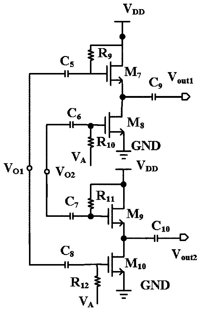
[0021] It includes an input matching network, a first-stage active balun circuit and a second-stage output active balun circuit; the input matching network adopts a π-type matching structure, and the first inductor L1 , the first capacitance C 1 , the feedback resistor R f and the feedback capacitor C f Together they form a feedback loop to form a 50-ohm input impedance match, while improving the isolation between ports. The first-stage active balun circuit and the second-stage output active balun circuit use a capacitor C 5 , C 6 , C 7 and C 8 Perform cross-coupling connection, the capacitive cross-coupling connection between the first-stage active balun circuit and the second-stage output active balun circuit refers to the seventh NMOS transistor M in the...


PUM


Abstract

According to the broadband CMOS second-order active balun amplifier, a series structure of two stages of active balun is used, higher phase precision is obtained, and the requirement for high loss ofa radio frequency circuit is met. Phase shift in the transmission process from a signal source to a load is eliminated through the input pi-type matching circuit, and 50-ohm input impedance matching is achieved; the first-stage active balun circuit and the second-stage output active balun circuit are in cross coupling connection through a capacitor, and the first-stage active balun circuit uses abroadband phase correction technology to obtain Vo1 and Vo2 with small phase errors and gain errors; according to the second-stage active balun circuit, two double-end-to-single-end baluns are used asoutput ends, a traditional source follower is replaced as a buffer, the phase precision is improved through phase compensation between signals, and meanwhile output matching is achieved. The invention can be used for an active balun amplifier of 1-8GHz.

Description

technical field [0001] The invention belongs to the technical field of microelectronics, and further relates to a broadband complementary metal oxide semiconductor CMOS (Complementary Metal Oxide Semiconductor) second-order active balun amplifier for L-C bands in the technical field of radio frequency integrated circuits. The invention can be used in the wireless communication system to realize the conversion between single-end and double-end signals, and at the same time provide certain power gain and better isolation of input and output, and ensure good balance of signals. Background technique [0002] Since the beginning of the 21st century, integrated circuit design technology has developed rapidly, various new digital and radio frequency circuits have become more and more widely used, and the digital transmission frequency requirements of transmitting / receiving communication modules are also getting higher and higher. In wireless communication systems such as radio freq...

Claims


Application Information

Patent Timeline
Patent Type & Authority Applications(China)
IPC IPC(8): H03F1/56
CPCH03F1/565
Inventor 李振荣程夏禹陈中姜国超李臻庄奕琪
Owner XIDIAN UNIV
Why Eureka
Try Eureka