Method and structure for improving working performance of pentacene organic field effect transistor

A transistor and pentacene technology, applied in the field of microelectronics, can solve the problems of not meeting industrial standards, pentacene organic field effect transistor devices have not been practically applied, etc., to improve programming/erasing reliability and data retention capability , the effect of improving work performance

Active Publication Date: 2020-05-15
NANJING UNIV
View PDF4 Cites 8 Cited by
  • Summary
  • Abstract
  • Description
  • Claims
  • Application Information

AI Technical Summary

Problems solved by technology

Program / erase operation of pentacene organic field effect devices with pulse voltages of such high pulse amplitudes or such long pulse widths does not meet industry standards for modern electronic device applications
Therefore, so far, pentacene organic field-effect transistor devices using polymer thin films as charge-trapping media have not been practically applied.

Method used


Image

  • Method and structure for improving working performance of pentacene organic field effect transistor
  • Method and structure for improving working performance of pentacene organic field effect transistor
  • Method and structure for improving working performance of pentacene organic field effect transistor

Examples


Embodiment 1

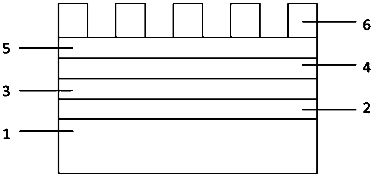
[0036] Embodiment 1 Structure gate electrode / insulating layer / polymer dielectric film / pentacene / source and drain electrodes of the traditional pentacene organic field effect transistor, the present invention sets an n-type between the polymer dielectric and pentacene Semiconductor film transition layer;

[0037] The polymer medium film has the effect of trapping charge, and the polymer medium is preferably PS, PVN, but not limited to these several, and its preparation method includes solution method, as spin-coating method (spin-coating), sol-gel method (sol-gel method). gel), or spraying method (spray), or screen printing method (silk-screen printing), ink-jet printing method (ink-jeting), etc., or thermal evaporation method, or other similar physical and chemical film preparation methods, which The thickness range is 1nm-100nm;

[0038] The n-type semiconductor transition layer can be an n-type inorganic semiconductor film, or an n-type organic semiconductor film;

[0039]...

Embodiment 2

[0057] The difference between this embodiment and embodiment 1 is that the charge trapping medium 3 is polystyrene (PS) with a thickness of 40 nm, and the preparation method still adopts the spin coating method.

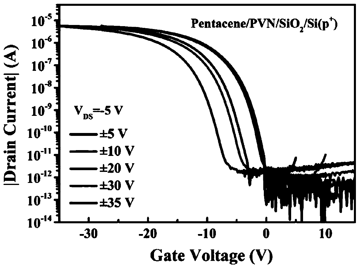
[0058] Image 6 It is the transfer characteristic curve of the pentacene organic field effect transistor with the PTCDI-C13 transition layer added in Example 2, wherein the gate voltage is -5V, and the source-drain voltage test range is ±30V~±40V, and it can be seen that the window increases with the voltage When the source-drain voltage is 35V, the window exceeds 17V, and the distinction between the on state and the off state is more obvious.

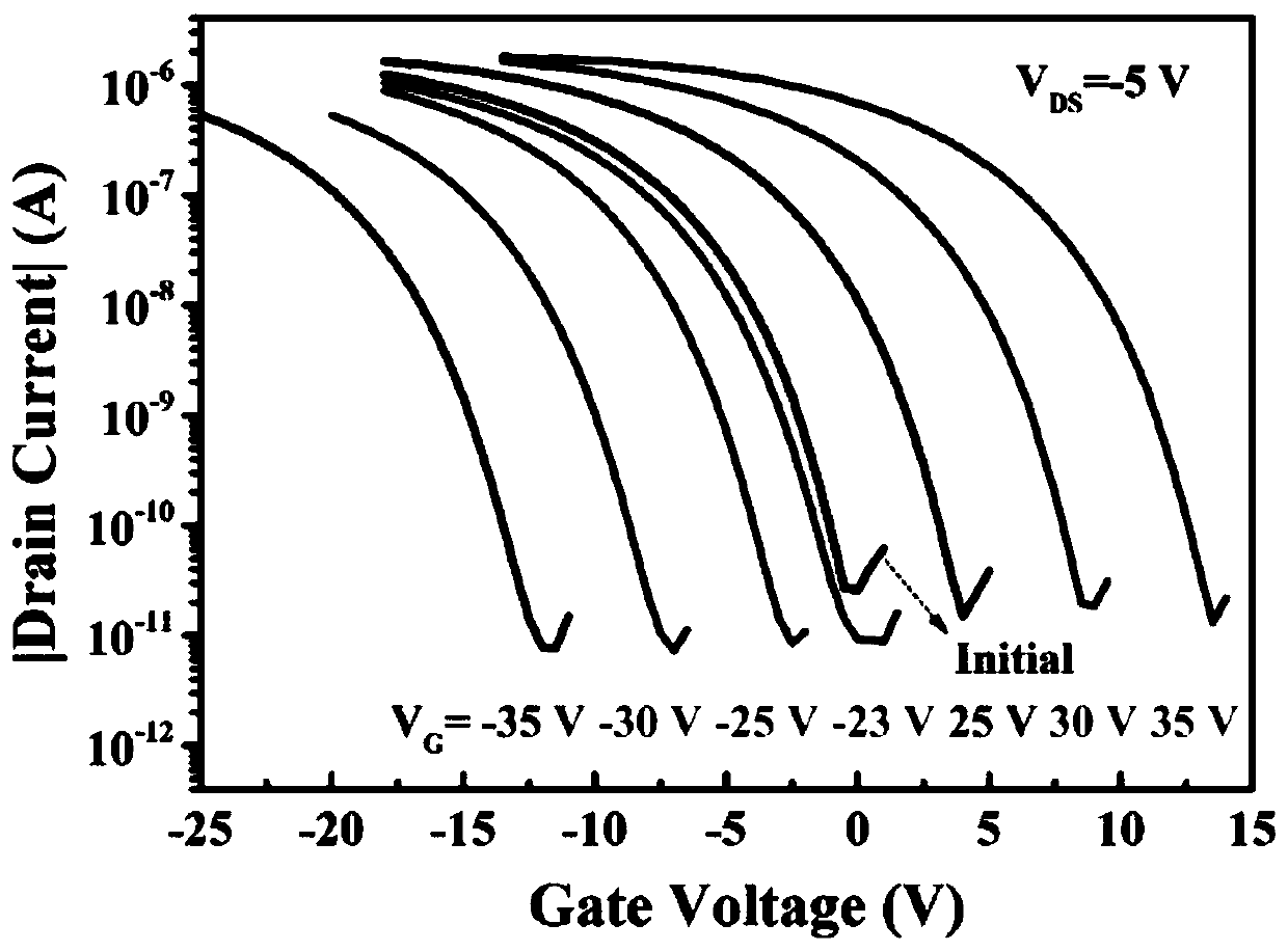
[0059] Figure 7 It is the transfer characteristic curve of pentacene organic field effect transistor without PTCDI-C13 transition layer. The gate voltage is -5V, and the voltage test range is ±5V~±35V. It can be seen that when the source-drain voltage is less than 25V, the curve There is almost no movement, and then the wi...

Embodiment 3

[0062] The difference between this embodiment and embodiment 1 is that the transition layer 4 of the n-type semiconductor thin film is zinc oxide (ZnO) with a thickness of 10 nm, and the preparation method adopts the magnetron sputtering method.

[0063] Figure 8 It is the transfer characteristic curve of the pentacene organic field effect transistor with ZnO transition layer added in Example 3, wherein the gate voltage is -5V, the source-drain voltage test range is ±5V~±40V, it can be seen that the window changes rapidly with the increase of voltage Large, when the source-drain voltage is 30V, the window is about 20V, and the distinction between the on state and the off state is more obvious.

[0064] Depend on Figure 8 image 3 It can be seen from the comparison that after adding the ZnO transition layer, the window of the device becomes significantly larger, and the transfer characteristics are significantly improved.


PUM

PropertyMeasurementUnit
thicknessaaaaaaaaaa
thicknessaaaaaaaaaa
thicknessaaaaaaaaaa

Abstract

The invention discloses a method for improving the working performance of a pentacene organic field effect transistor, and the method comprises the steps of setting an n-type semiconductor film transition layer between a polymer medium and pentacene in an organic field effect transistor device which is of a gate electrode / insulating layer / polymer medium film / pentacene / source and drain electrode structure, wherein the thickness of the n-type semiconductor transition layer is 1-100 nm; reducing the hole barrier height at an interface of pentacene and a charge trapping medium through the inducedelectrons at an interface in the n-type semiconductor transition layer so as to reduce a programming / erasing working voltage of the pentacene organic semiconductor transistor effectively; preventing the positive charges (holes) captured in the polymer dielectric film from escaping into a pentacene film through a positively charged space charge region formed by the ionization donors in the organicsemiconductor transition layer, so that the programming / erasing reliability and the data retention capability of the pentacene organic semiconductor transistor device are improved, and the working performance of the pentacene organic field effect transistor is improved.

Description

technical field [0001] The invention belongs to the technical field of microelectronics, and in particular relates to a method and application for improving the working performance of pentacene organic field-effect transistors Background technique [0002] Nonvolatile electronic devices based on organic field-effect transistors have received a lot of attention over the past two decades due to their promising applications in fields ranging from radio frequency identification tags to flexible and large-area displays [1,2]. In order to promote the practical application of organic field effect devices, a lot of effort has been spent on researching charge-trapping materials such as p-type channel materials, n-type channel materials and polymers. As one of the most potential p-type channel materials, the small molecule semiconductor material pentacene (pantacene) with a planar molecular structure of five benzene rings has been widely used in the structural research of organic semi...

Claims


Application Information

Patent Timeline
Patent Type & Authority Applications(China)
IPC IPC(8): H01L51/05H01L51/10H01L51/30H01L51/40
CPCH10K71/00H10K85/111H10K10/46H10K10/80H10K85/141H10K10/471
Inventor 康利民王一如殷江夏奕东
Owner NANJING UNIV
Why Eureka
Try Eureka