Ultraviolet led epitaxial structure and preparation method thereof
An epitaxial structure, ultraviolet technology, applied in the direction of semiconductor devices, electrical components, circuits, etc., can solve the problems affecting the luminous efficiency and service life of ultraviolet LEDs
- Summary
- Abstract
- Description
- Claims
- Application Information
AI Technical Summary
Problems solved by technology
Method used
Image
Examples
preparation example Construction
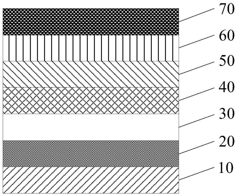
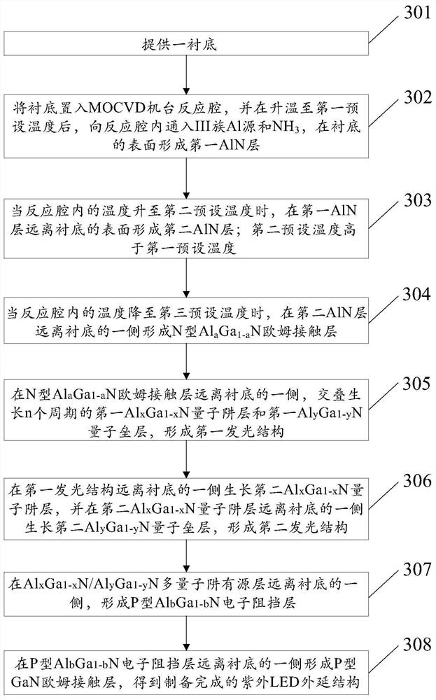
[0077] image 3 Shown is a flow chart of the method for preparing the ultraviolet LED epitaxial structure provided by the embodiment of the present application. See figure 1 and image 3 , the present application also provides a method for preparing an ultraviolet LED epitaxial structure, the method comprising:
[0078] Step 301, providing a substrate 10;
[0079]Step 302, put the substrate 10 into the reaction chamber of the MOCVD machine, and after heating up to the first preset temperature, feed the group III Al source and NH into the reaction chamber 3 , forming a first AlN layer 20 on the surface of the substrate; optionally, the first preset temperature range is 600°C-1000°C.
[0080] Step 303, when the temperature in the reaction chamber rises to a second preset temperature, a second AlN layer 30 is formed on the surface of the first AlN layer 20 away from the substrate 10; the second preset temperature is higher than the first preset temperature; Optionally, the s...
Embodiment 1
[0088] Step 1, put the sapphire substrate into the reaction chamber of the MOCVD machine, and pass TMAl, NH 3 and H 2 , forming a low-temperature AlN layer with a thickness of 25 nm on the surface of the sapphire substrate.
[0089] Step 2, at 1270°C, feed TMAl, NH under the reaction chamber pressure of 50Torr 3 and H 2 , forming a high-temperature AlN layer with a thickness of about 3 μm.
[0090] Step 3, lower the temperature to 1070°C, and feed TMAl, TMGa, SiH under the pressure of 50Torr in the reaction chamber 4 , NH 3 and H 2 , forming N-type Al with a thickness of about 2 μm a Ga 1-a N ohmic contact layer; where, SiH 4 It is N-type dopant, Si concentration is 1.5E+19cm -3 .
[0091] Step 4, lower the temperature to 1000°C, and feed TMAl, TMGa, SiH under the pressure of 50Torr in the reaction chamber 4 , NH 3 and H 2 , forming the first Si-doped Al x Ga 1-x N quantum well layer, the thickness is about 2nm, the Al composition is about 44%, and the doping co...
PUM
| Property | Measurement | Unit |
|---|---|---|
| thickness | aaaaa | aaaaa |
| thickness | aaaaa | aaaaa |
Abstract
Description
Claims
Application Information


