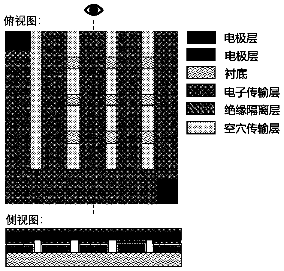
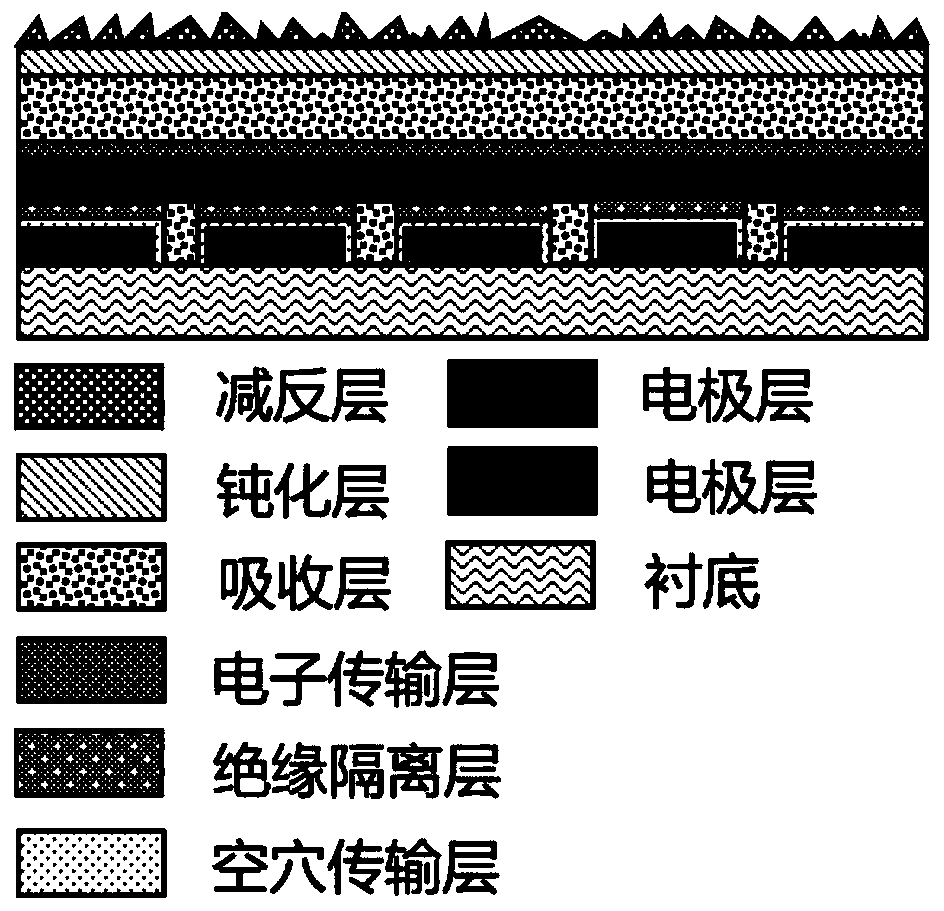
Positive interdigital full-back contact perovskite solar cell and preparation method thereof
A full-back contact and solar cell technology, applied in the field of solar cells, can solve problems such as limiting solar cell collection efficiency, hindering solar cell conversion efficiency, metal electrode shading, etc., to reduce costs, improve light utilization, and reduce reflections Effect
- Summary
- Abstract
- Description
- Claims
- Application Information
AI Technical Summary
Problems solved by technology
Method used
Image
Examples
Embodiment 1
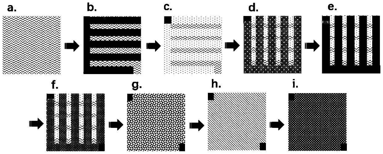
[0025] 1) Use glass as the substrate, and use ultrasonic and electronic cleaning fluid to clean it, such as image 3 a;
[0026] 2) Prepare a comb-shaped copper film with a thickness of 200nm by magnetron sputtering and a mask plate, such as image 3 b;
[0027] 3) Using evaporation deposition method and mask plate in image 3 Prepare a hole transport layer on the left comb electrode in b, such as Spiro-TPD, with a thickness of 100nm, such as image 3 c;
[0028] 4) Prepare dense SiO with a thickness of 100 nm on the hole transport layer by thermal evaporation and mask 2 film, such as image 3 d;
[0029] 5) Prepare a comb-shaped copper film with a thickness of 200nm by magnetron sputtering and a mask plate, such as image 3 e;
[0030] 6) Using thermal evaporation method and mask plate in image 3 Prepare an electron transport layer on the comb electrode in e, such as PCBM, with a thickness of 50nm, such as image 3 f;
[0031] 7) Prepare a polycrystalline perovski...
Embodiment 2
[0036] 1) Use glass as the substrate, and use ultrasonic and electronic cleaning fluid to clean it, such as image 3 a;
[0037] 2) Prepare a comb-shaped copper film with a thickness of 100nm by thermal evaporation method and mask plate, such as image 3 b;
[0038] 3) Using magnetron sputtering method and mask plate in image 3 Prepare a hole transport layer on the comb electrode in b, such as NiO x , thickness 100nm, such as image 3 c;
[0039] 4) Prepare dense SiO with a thickness of 100 nm on the hole transport layer by magnetron sputtering and mask 2 film, such as image 3 d;
[0040] 5) Prepare a comb-shaped titanium film with a thickness of 100nm by thermal evaporation method and mask plate, such as image 3 e;
[0041] 6) Using magnetron sputtering method and mask plate in image 3 Preparation of electron transport layer on the comb electrode in e, such as TiO 2 , thickness 50nm, such as image 3 f;
[0042] 7) Prepare a polycrystalline perovskite absorbi...
Embodiment 3
[0047] 1) Use glass as the substrate, and use ultrasonic and electronic cleaning fluid to clean it, such as image 3 a;
[0048] 2) adopt magnetron sputtering method and mask plate to prepare the comb gold film of thickness 50nm, as image 3 b;
[0049] 3) Prepare dense Al with a thickness of 20 nm on the hole transport layer by chemical vapor deposition and mask 2 o 3 film, such as image 3 d;
[0050] 4) Prepare a comb-shaped titanium film with a thickness of 100nm by thermal evaporation and a mask, such as image 3 e;
[0051] 5) Prepare a polycrystalline perovskite absorbing layer with a thickness of 700nm by one-step solution spin coating method, such as image 3 g;
[0052] 6) Prepare a KI passivation layer with a thickness of 15nm by thermal evaporation, such as image 3 h;
[0053] 7) Preparation of SiO with low refractive index by electron beam evaporation 2 / MgF 2 Dense anti-reflection protective layer with a thickness of 100nm, such as image 3 i.
[0...
PUM
| Property | Measurement | Unit |
|---|---|---|
| thickness | aaaaa | aaaaa |
| thickness | aaaaa | aaaaa |
| width | aaaaa | aaaaa |
Abstract
Description
Claims
Application Information


