AlGaAs/GaAs high-electron-mobility transistor with multi-channel laminated insulation side gate fin type structure and preparation method thereof

A technology with high electron mobility and fin structure, which is applied in the field of microelectronics, can solve problems such as gate leakage, and achieve the effects of improving device transconductance, improving device transconductance and device gain capabilities, and high current drive capabilities

Active Publication Date: 2020-07-17
SHANGHAI SPACEFLIGHT INST OF TT&C & TELECOMM
View PDF8 Cites 2 Cited by
  • Summary
  • Abstract
  • Description
  • Claims
  • Application Information

AI Technical Summary

Problems solved by technology

[0004] However, the linear operating characteristics of the existing fin-type devices need to be further improved, and there is also the problem of gate leakage due to the introduction of the fin-type side gate structure

Method used


Image

  • AlGaAs/GaAs high-electron-mobility transistor with multi-channel laminated insulation side gate fin type structure and preparation method thereof
  • AlGaAs/GaAs high-electron-mobility transistor with multi-channel laminated insulation side gate fin type structure and preparation method thereof
  • AlGaAs/GaAs high-electron-mobility transistor with multi-channel laminated insulation side gate fin type structure and preparation method thereof

Examples


Embodiment 1

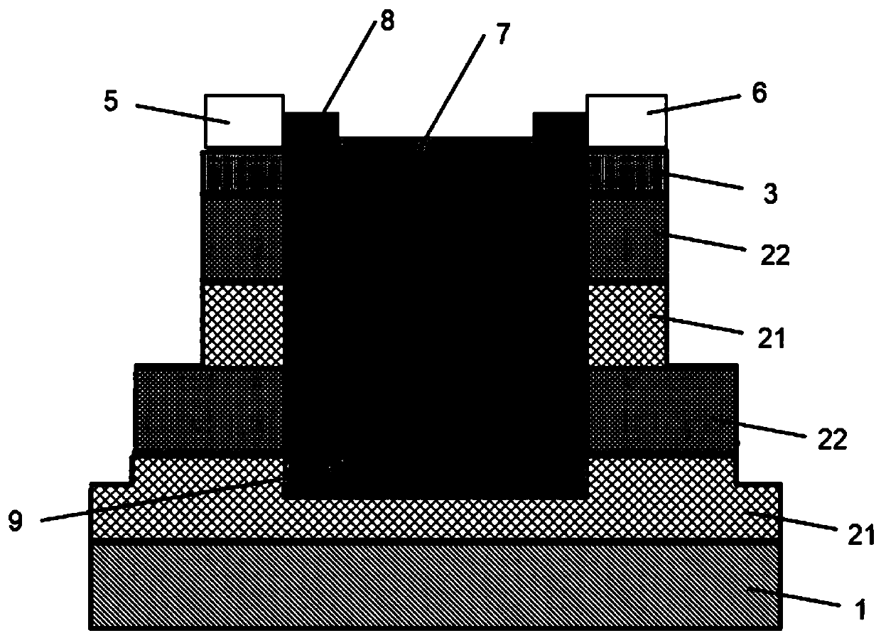
[0057] see Figure 1 to Figure 3 As shown, will figure 1 The A-A' direction is defined as the end face of the high electron mobility transistor, and the BB' direction is defined as the side surface of the high electron mobility transistor. This embodiment provides a multi-channel stacked insulating side gate fin type structure AlGaAs / GaAs high electron mobility transistor, including GaAs or germanium substrate 1, several layers of AlGaAs / GaAs heterojunction 2, GaAs cap layer 3, SiN passivation layer 4, source electrode 5, leakage current transistor from bottom to top Pole 6 and gate electrode 7;

[0058] The AlGaAs / GaAs heterojunction 2 includes a GaAs layer 21 and an AlGaAs barrier layer 22, and the GaAs layer 21 is close to the GaAs or germanium substrate 1. The high electron mobility transistor provided by the present invention includes a multilayer AlGaAs / GaAs heterojunction 2, Multiple parallel two-dimensional electron gas pathways can be formed between the source and d...

Embodiment 2

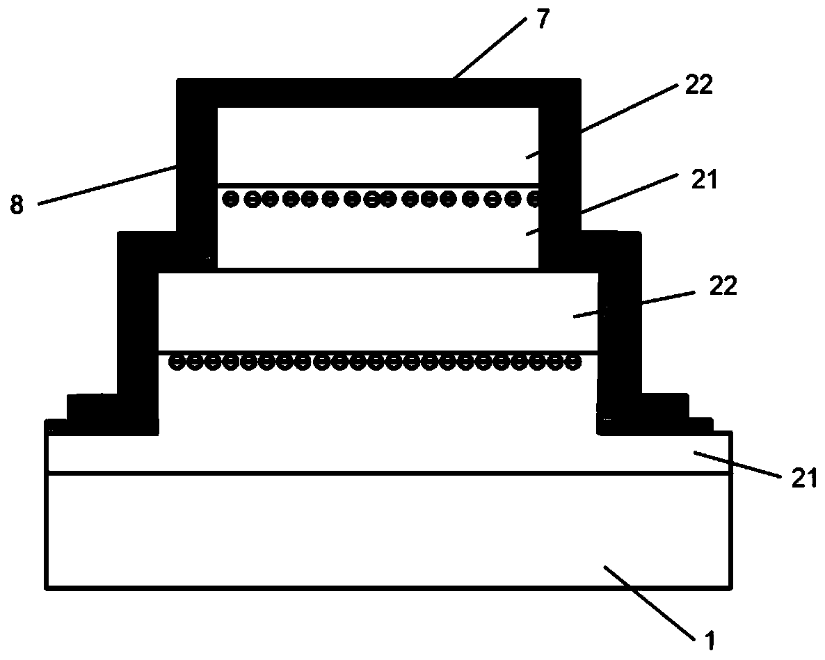
[0067] see Figure 4 to Figure 15 As shown, based on the same inventive concept, this embodiment provides a method for preparing an AlGaAs / GaAs high electron mobility transistor with a multi-channel stacked insulating side-gate fin structure, including the following steps:

[0068] S1: see Figure 5 As shown, a GaAs or germanium substrate 1 is provided first, and then a GaAs layer 21 and an AlGaAs barrier layer 22 are sequentially grown on the GaAs or germanium substrate 1 by MOCVD process to form the first layer of AlGaAs / GaAs heterojunction 2, Wherein, the thickness of the AlGaAs barrier layer 22 is 15-25 nm, and the Al composition in the AlGaAs barrier layer 22 is 25-35%;

[0069] S2: see Image 6 As shown, step S1 is repeated several times on the first layer of AlGaAs / GaAs heterojunction 2 to obtain several layers of AlGaAs / GaAs heterojunction 2 to form a multi-channel structure, wherein the thickness of the AlGaAs barrier layer 22 is 15- 25nm, the Al composition in the...

Embodiment 3

[0083] This embodiment provides a method for preparing an AlGaAs / GaAs high electron mobility transistor with a multi-channel stacked insulating side-gate fin structure, which specifically includes the following steps:

[0084] Step 1. Epitaxial material growth.

[0085] 1.1) On the germanium substrate, the intrinsic GaAs layer is grown by MOCVD process;

[0086] 1.2) On the intrinsic GaAs layer, grow a 15nm-thick AlGaAs barrier layer, wherein the Al composition is 35%, and the doping concentration is 4×10 17 cm -3 , forming a 2DEG at the contact position between the intrinsic GaAs layer and the AlGaAs barrier layer;

[0087] 1.3) growing a second intrinsic GaAs layer on a 15nm thick AlGaAs barrier layer;

[0088] 1.4) A second 15nm thick AlGaAs barrier layer is grown on the second intrinsic GaAs layer, wherein the Al composition is 35%, and the doping concentration is 4×10 17 cm -3 , forming a heterojunction material structure with double channels.

[0089] 1.5) A highly...


PUM

PropertyMeasurementUnit
widthaaaaaaaaaa
thicknessaaaaaaaaaa
thicknessaaaaaaaaaa

Abstract

The invention discloses an AlGaAs / GaAs high-electron-mobility transistor with a multi-channel laminated insulation side gate fin type structure. The AlGaAs / GaAs high-electron-mobility transistor sequentially comprises a GaAs or germanium substrate, a plurality of layers of AlGaAs / GaAs heterojunctions, a GaAs cap layer, a SiN passivation layer, a source electrode, a drain electrode and a gate electrode from bottom to top, wherein the gate fin adopts a laminated structure with different fin widths at the upper and lower layers, the fin width of the upper layer being smaller than that of the lower layer; and an insulating dielectric layer is arranged between the gate electrode and the side walls of the plurality of layers of AlGaAs / GaAs heterojunctions. The high-electron-mobility transistor provided by the invention adopts a three-dimensional laminated fin type structure, so that gate regions with different fin widths perform composite control on a device channel, which is equivalent to parallel connection of devices with different threshold values; when gate voltage is applied, transconductance performance of the device is widened and linear working characteristics are improved; theinsulating dielectric layer is introduced into the side wall of the gate fin, so that the leakage current introduced by the side gate etching surface of the fin type structure is effectively reduced,the static power consumption of the device is reduced, and the breakdown voltage of the device is improved.

Description

technical field [0001] The invention belongs to the technical field of microelectronics, and in particular relates to an AlGaAs / GaAs high electron mobility transistor with a multi-channel stacked insulating side gate fin structure and a preparation method thereof. Background technique [0002] High electron mobility transistors (HEMTs) are recognized as one of the most promising high-speed electronic devices. Because of its characteristics of ultra-high speed, low power consumption, and low noise (especially at low temperature), it can meet the needs of ultra-high-speed computers, signal processing, satellite communications, etc., and thus has been widely valued. As a new generation of microwave and millimeter wave devices, high electron mobility transistors (HEMTs) show unparalleled advantages in terms of frequency, gain and efficiency. GaAs / Al x Ga 1-x As material is the material system with the earliest development, the widest application and the most research. Since t...

Claims


Application Information

Patent Timeline
Patent Type & Authority Applications(China)
IPC IPC(8): H01L29/778H01L29/40H01L29/423H01L21/335
CPCH01L29/7783H01L29/404H01L29/42356H01L29/66462
Inventor 陈凯化宁沈晓唯章泉源王佳尚会锋姚崇斌王茂森张瑞珏戴杰黄硕
Owner SHANGHAI SPACEFLIGHT INST OF TT&C & TELECOMM
Why Eureka
Try Eureka