Preparation method of tunneling oxidation passivation battery

A tunneling and battery technology, applied in the field of solar photovoltaic, can solve the problems of long process flow and poor appearance, and achieve the effect of simplifying the process, improving passivation performance and saving costs.

Inactive Publication Date: 2020-08-11
CHANGZHOU UNIV +1
View PDF6 Cites 3 Cited by
  • Summary
  • Abstract
  • Description
  • Claims
  • Application Information

AI Technical Summary

Problems solved by technology

[0004] The purpose of the present invention is to solve the technical problems of long technological process in the prior art and poor appearance during plating and cleaning, and to provide a new type of preparation process for tunneling oxidation passivation cells. Doping and growing a thick oxide mask layer simplifies the process flow, reduces labor and equipment costs, and improves the uniformity of doping. At the same time, due to the thicker oxide layer, the heat is more uniform in the subsequent annealing process, effectively improving Uniformity after doping

Method used


Image

  • Preparation method of tunneling oxidation passivation battery
  • Preparation method of tunneling oxidation passivation battery
  • Preparation method of tunneling oxidation passivation battery

Examples


Embodiment 1

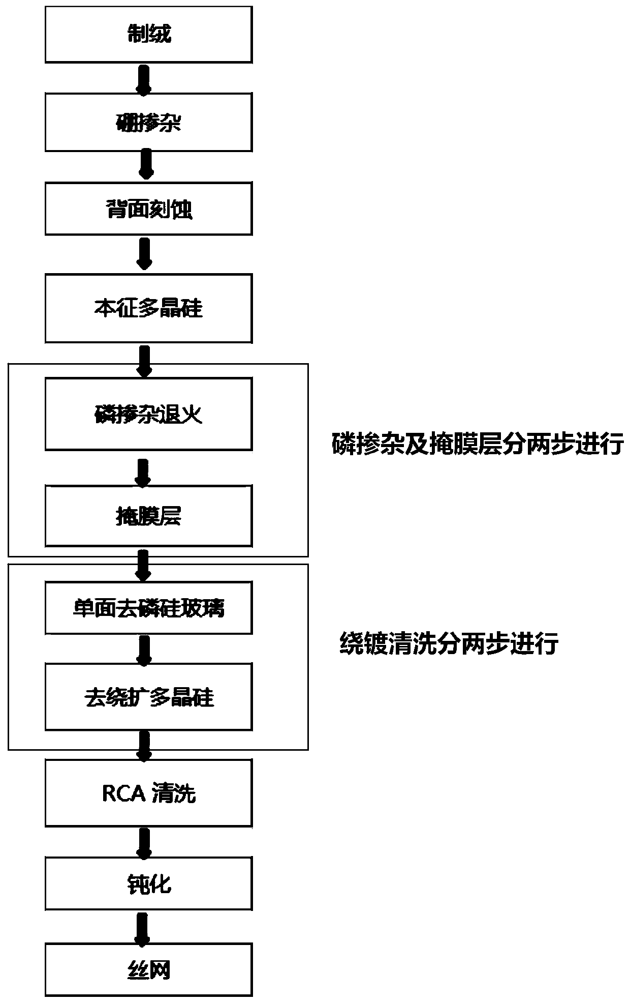
[0035] The preparation process steps of a novel tunneling oxidation passivation battery are as follows:

[0036] (1) Polishing—Using N-type silicon wafers as the substrate, using a slot machine KOH: polishing additive: H 2 O=2:1:15 (volume ratio) (polishing additive is composed as follows according to the mass fraction: 4 parts of sodium benzoate, 7 parts of surfactant (sodium hydroxide: alkylphenol polyoxyethylene ether=1:2 (mass ratio)), 11 parts of palmitic acid, 3 parts of polyethylene glycol, 2 parts of alkyl polyglucoside and 73 parts of deionized water), the temperature is controlled at 75°C, the polishing time is 6min, the weight loss is 0.7g, and the reflectivity is controlled at 38%;

[0037] (2) Doped polysilicon—in the LPCVD furnace tube, the silicon oxide deposition temperature is maintained at 610°C, O 2 (Oxygen) 2L, time 20min, thickness 1.4nm; followed by intrinsic polysilicon deposition, deposition temperature 620°C, SiH 4 (Silane) flow rate 500sccm, time 2...
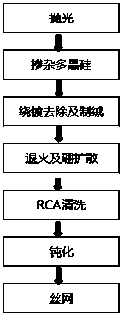
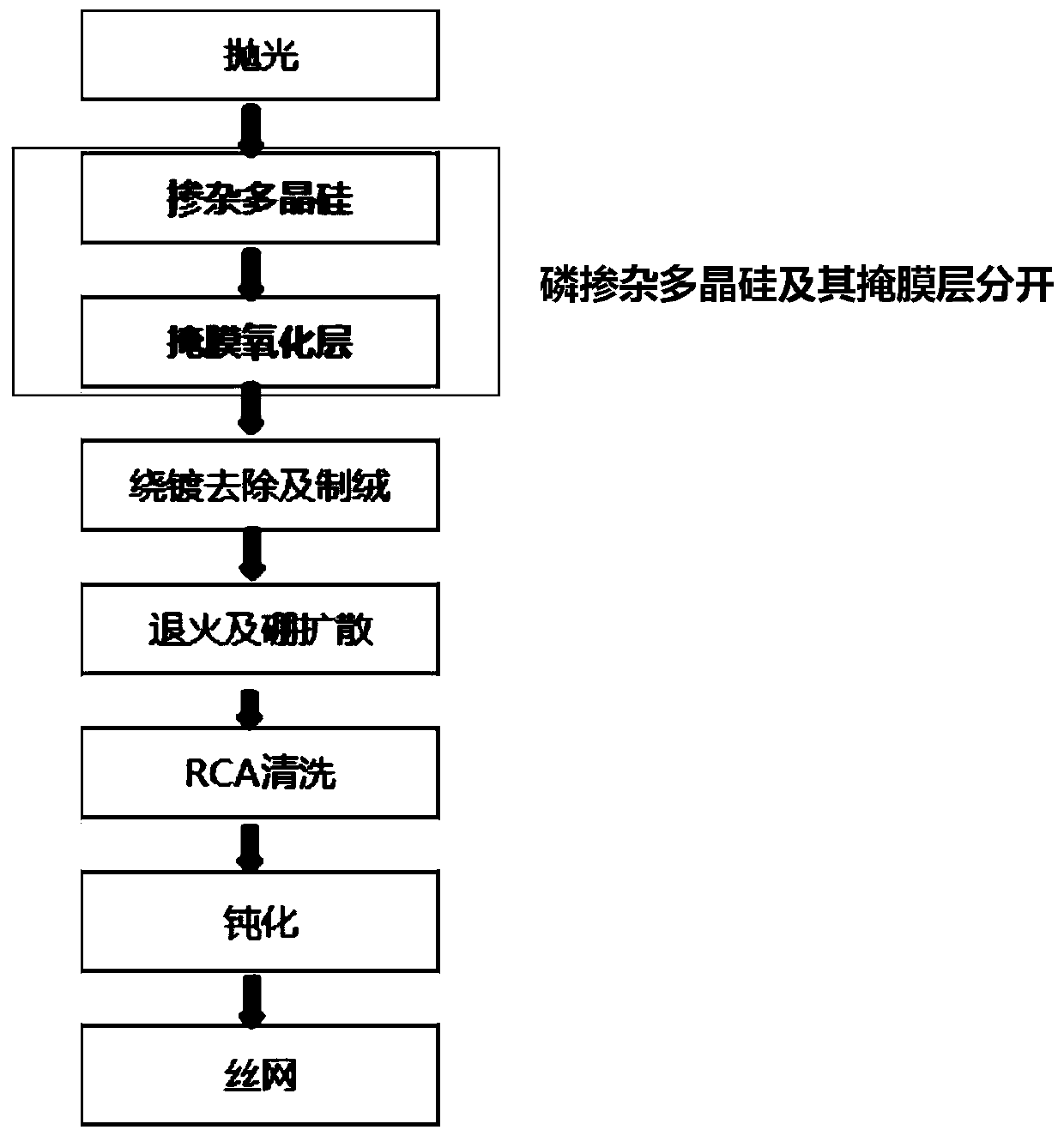
Embodiment 2

[0045] (1) Polishing - using N-type silicon wafer as the substrate, using NaOH: polishing additive: H 2 O=3:2:15 (volume ratio) chain polishing (polishing additive is composed as follows according to the mass fraction: 5 parts of sodium benzoate, 5 parts of surfactant (sodium hydroxide: alkylphenol polyoxyethylene ether=1: 1.5 (mass ratio)), 7 parts of palmitic acid, 3 parts of polyethylene glycol, 5 parts of alkyl polyglucoside and 75 parts of deionized water), the temperature is controlled at 80°C, the polishing time is 3min, the weight loss is 0.4g, and the reflection The rate is controlled at 39%;

[0046] (2) Doped polysilicon—in the LPCVD furnace tube, the silicon oxide deposition temperature is maintained at 620°C, O 2 (Oxygen) 1.5L, time 15min, thickness 1.6nm; followed by intrinsic polysilicon deposition, deposition temperature 610°C, SiH 4 (Silane) flow rate 550sccm, time 2min; repass SiH 4 450sccm, pH of 5% mass concentration 3 40sccm, time 40min, doped polysil...


PUM

PropertyMeasurementUnit
Thicknessaaaaaaaaaa
Thicknessaaaaaaaaaa
Thicknessaaaaaaaaaa

Abstract

The invention belongs to the field of solar photovoltaic industry and particularly relates to a preparation method of a tunneling oxidation passivation battery. The method is characterized in that a back surface adopts a polished surface structure so that the light utilization rate can be effectively improved, and the process steps are reduced by adopting one-step deposition of polycrystalline silicon phosphorus doping and growth of a thick oxidation mask layer; a whole surface of the coating is removed, the process window is enlarged, the defect of difficulty in removing the winding plating,namely the defect of difficulty in removing the winding plating due to the fact that boron diffusion is performed on a front surface and polycrystalline silicon is doped on a back surface in the conventional common process flow, is avoided, a certain mark is certainly caused even if the winding plating is completely removed, so the appearance yield is influenced. The method is advantaged in that an annealing and boron doping two-in-one mode is introduced into the method, so the process is simplified, the appearance is not poor, the process flow is short, energy consumption is low, the production yield is effectively increased, production quality is effectively improved, and the like.

Description

technical field [0001] The invention belongs to the field of solar photovoltaic industry, and in particular relates to a preparation method of a novel tunneling oxidation passivation battery. Background technique [0002] The pursuit of high-efficiency cells is the development trend in the photovoltaic industry, and the cost and process solutions are considered. At present, the mainstream product is still PERC (passivated emitter back surface full diffusion) cells, but its efficiency is already a bottleneck, and a new type of cell has been introduced. Cell structure, tunneling oxidation passivation contact cell. This structure provides good surface passivation for the back of the silicon wafer. The ultra-thin oxide layer can allow many electrons to tunnel into the polysilicon layer while blocking the recombination of minority electrons and holes, and then the electrons are transported laterally in the polysilicon layer and collected by the metal, thus greatly The metal cont...

Claims


Application Information

Patent Timeline
IPC IPC(8): H01L31/18
CPCH01L31/1804H01L31/186H01L31/1864H01L31/1868Y02E10/547Y02P70/50
Inventor 袁宁一王芹芹丁建宁程广贵王书博
Owner CHANGZHOU UNIV
Why Eureka
Try Eureka