Photoresist-free photoinduced patterning method of quantum dot film

A quantum dot and patterning technology, applied in the field of photoresist-free photopatterning, can solve the problems of unfavorable high-resolution, high-performance patterned quantum dot films, etc., and achieve a wide range of applications, easy application, and high photoluminescence. The effect of efficiency

Active Publication Date: 2020-10-16
TSINGHUA UNIV
View PDF4 Cites 2 Cited by
  • Summary
  • Abstract
  • Description
  • Claims
  • Application Information

AI Technical Summary

Problems solved by technology

For example, the traditional photolithography technology based on photoresist template is one of the most important technologies in the field of integrated circuit microfabrication, but

Method used


Image

  • Photoresist-free photoinduced patterning method of quantum dot film
  • Photoresist-free photoinduced patterning method of quantum dot film
  • Photoresist-free photoinduced patterning method of quantum dot film

Examples


Example Embodiment

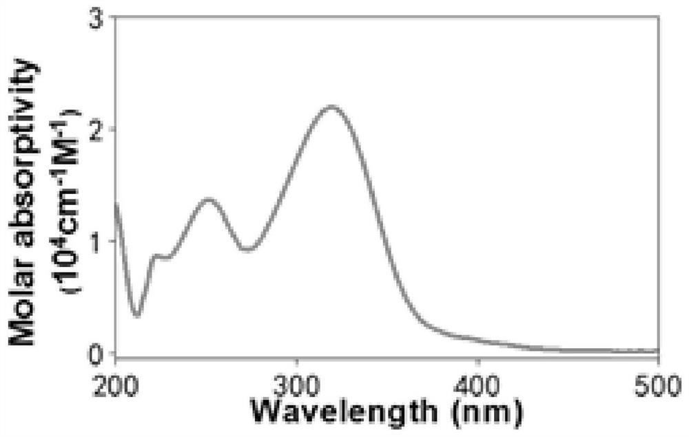
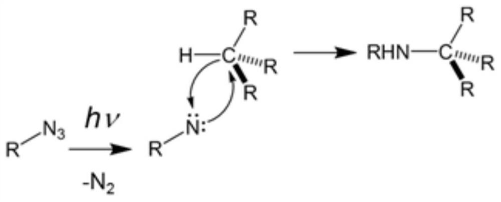
[0055] Synthesis of embodiment 1 photosensitive crosslinking molecule

[0056] Add 358 mg of sodium azide and 980 mg of pentafluorobenzaldehyde into a double-neck round bottom flask connected with a reflux condenser, pour 7.5 mL of acetone and 7.5 mL of water. The reaction solution was stirred and heated to reflux for 18 hours under the protection of nitrogen. After the reaction, the product was cooled to room temperature, and then 25 mL of water was added to dilute the initial reaction mixture, followed by extraction with 25 mL of ether, which was repeated three times. The organic layer was washed with saturated brine, dried over magnesium sulfate to remove water, and then distilled under reduced pressure to obtain a concentrated solution. Then it was purified by silica gel chromatography, and the eluent was a mixed solvent of ethyl acetate and n-hexane (volume fraction of ethyl acetate was 5%). After recrystallization from n-hexane, 680 mg of white solid 4-azido-2,3,5,6-te...

Example Embodiment

[0058] Embodiment 2 patterning process

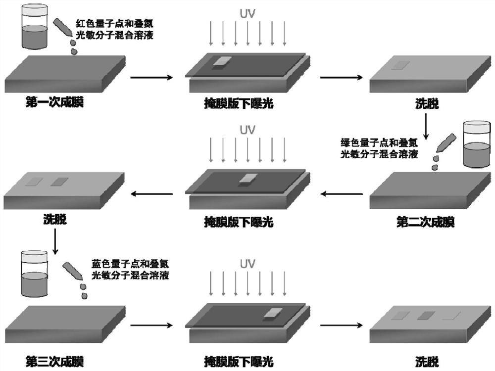
[0059] Using the method disclosed in the existing literature to synthesize CdSe / ZnS core-shell quantum dots emitting red light, the patterning process is as follows:

[0060] In order to avoid the influence of external ultraviolet light on the patterning process, the following operations must be performed under yellow light:

[0061] 1) Quantum dot film preparation: disperse the synthesized red CdSe / ZnS quantum dots in toluene, add the photosensitive crosslinking molecule (3E,5E)-3,5-bis(4-azido-2) synthesized in Example 1 ,3,5,6-Tetrafluorobenzylidene)-1-methylpiperidin-4-one, and stir and mix evenly, the quantum dot concentration is 30mg / mL, (3E,5E)-3,5- The molecular concentration of bis(4-azido-2,3,5,6-tetrafluorobenzylidene)-1-methylpiperidin-4-one is 2.5mg / mL, that is, quantum dots and photosensitive cross-linked molecules The mass ratio is 100:12.

[0062] Silicon is used as the substrate to prepare the quantum dot film. The sub...

Example Embodiment

[0066] Example 3

[0067] Same as the patterning method of Example 2, the difference is that the quantum dots used are CdSe, and the optical microscope photo of the quantum dot film made in this embodiment is shown in Figure 5 a.


PUM


Abstract

The invention discloses a photoresist-free photoinduced patterning method of a quantum dot film, and the method comprises the following steps: a, dispersing quantum dots in a non-polar solvent, and adding photosensitive crosslinking molecules to prepare a film; b, exposing the film obtained in the step a under the irradiation of 365 nm ultraviolet light, and carrying out a cross-linking reaction;c, performing eluting by adopting a non-polar solvent to remove the quantum dots in the exposure area which is not irradiated by the ultraviolet light to obtain the patterned quantum dot film. The method provided by the invention is universally applicable to patterning of various quantum dot films with different components, properties and structures; the pattern resolution can reach below 10 microns; the resolution ratio is similar to that of a traditional photoetching technology and is superior to that of a quantum dot thin film obtained through a printing method, and the obtained thin film containing red, green and blue quantum dots of different colors has high photoluminescence efficiency and can be applied to display devices such as LEDs and other photoelectric devices based on quantumdots.

Description

technical field [0001] The invention belongs to the technical field of optoelectronic materials, and particularly relates to a photoresist-free photopatterning method for quantum dot films. Background technique [0002] Colloidal quantum dots are inorganic semiconductor materials synthesized by solution method and exhibiting quantum confinement effect. Quantum dots have unique physical and chemical properties and the characteristics of solution processability, and have important application prospects in many fields, especially in optoelectronic materials and devices. The excellent narrow-spectrum emission and broad-spectrum absorption properties make quantum dot films show great application potential in LED displays, solar cells, photodetectors, and other fields. [0003] A key to realizing quantum dot films from single prototype components to complex integrated array optoelectronic devices that meet application requirements is to develop controllable, efficient, and high-p...

Claims


Application Information

Patent Timeline
IPC IPC(8): G03F7/20C09K11/88C09K11/70C09K11/66C09K11/56C09K11/02
CPCC09K11/025C09K11/565C09K11/661C09K11/70C09K11/883G03F7/2004
Inventor 张昊李景虹卢少勇
Owner TSINGHUA UNIV
Why Eureka
Try Eureka