Manufacturing method of silicon-based deep hole microstructure

A manufacturing method and microstructure technology, applied in the direction of microstructure technology, microstructure devices, manufacturing microstructure devices, etc., can solve the problems of high cost, discomfort, and inability to accurately control the size of microstructures, and achieve low-cost effects

Pending Publication Date: 2020-10-23
CHANGCHUN INST OF OPTICS FINE MECHANICS & PHYSICS CHINESE ACAD OF SCI
View PDF0 Cites 4 Cited by
  • Summary
  • Abstract
  • Description
  • Claims
  • Application Information

AI Technical Summary

Problems solved by technology

At present, there are generally micro-nano processing methods such as electron beam exposure, focused ion beam etching, and nanoimprinting to obtain microstructured silicon-based materials, which are expensive and not suitable for large-scale production; in addition, using femtosecond laser Such as black silicon materials made by other means, also face the problem of not being able to precisely control the size of the microstructure

Method used


Image

  • Manufacturing method of silicon-based deep hole microstructure
  • Manufacturing method of silicon-based deep hole microstructure
  • Manufacturing method of silicon-based deep hole microstructure

Examples


Embodiment Construction

[0019] The present invention will be described in more detail below in conjunction with the accompanying drawings and embodiments.

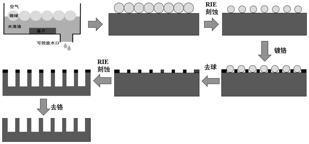
[0020] The production process is attached image 3 Shown:

[0021] Step 1: Cleaning, the thickness of the silicon wafer is 100-500um, and the surface of the silicon wafer is cleaned. In order to enhance the hydrophilicity of the surface of the silicon wafer, first put the silicon wafer into hydrogen peroxide and ammonia water for ten minutes each, and then clean it with distilled water and place it clean place to dry

[0022] Take a petri dish with a diameter of 10 cm and clean it with distilled water first, then put the petri dish into an ultrasonic instrument for ultrasonic cleaning for 1 hour, take it out and put it in a clean place to dry.

[0023] Step 2: Configure polystyrene microsphere solution, microsphere suspension in deionized water, its concentration is 5.0-10.0wt%, select the original solution of microspheres with a suitable size ...


PUM

PropertyMeasurementUnit
Thicknessaaaaaaaaaa

Abstract

A manufacturing method of a silicon-based deep-hole microstructure comprises the following steps: firstly, sequentially putting a silicon wafer into hydrogen peroxide and ammonia water, respectively soaking for 10 minutes, then cleaning with distilled water, putting in a clean place, and airing for later use; preparing turbid liquid in microsphere deionized water, selecting an original microspheresolution with an appropriate size of 400nm-100mu m, adding ethanol of which the volume is twice of that of the original microsphere solution, and performing ultrasonic treatment in an ultrasonic instrument for half an hour, so that polystyrene and ethanol are uniformly mixed; enabling the microspheres to form single-layer ordered arrangement on the liquid level; transferring the arranged microspheres to a silicon wafer by using a liquid level sedimentation method; reducing the sizes of the microspheres to obtain specific sizes; depositing 10-20 nm chromium metal on the etched sample wafer through a coating technology, and removing microspheres to form a microstructure with a hole array on a chromium film; and taking the chromium film with the hole array as a mask, removing the chromium film after etching, and finally manufacturing the silicon-based deep hole microstructure. A simple, efficient, large-area and low-cost method is provided for microstructuring the silicon-based material.

Description

technical field [0001] The invention relates to the technical field of semiconductor materials, in particular to a method for making a deep-hole microstructure on a silicon base. Background technique [0002] As we all know, silicon material is the most widely used semiconductor material in the world. Compared with other semiconductor materials, silicon materials have the following outstanding advantages: First, the silicon element reserves are huge, wafer silicon processing is convenient, the mechanical properties are good, and the cost is lower compared with other semiconductor materials; Transparent, it is very suitable as a transmission waveguide in certain wavelength bands; third, silicon-based optoelectronic technology is highly compatible with the current mature complementary metal oxide semiconductor process, and the accumulation of technical experience is very sufficient. Due to the above factors, silicon-based semiconductor devices have advantages that many non-si...

Claims


Application Information

Patent Timeline
IPC IPC(8): H01L21/3065B81C1/00
CPCH01L21/3065B81C1/00619B81C1/00531B81C1/00396B81C1/00404
Inventor 李强李资政王笑夷杨海贵高劲松
Owner CHANGCHUN INST OF OPTICS FINE MECHANICS & PHYSICS CHINESE ACAD OF SCI
Why Eureka
Try Eureka