Interdigital back contact heterojunction solar cell based on LPCVD high-efficiency amorphous silicon doping technology

A solar cell and amorphous silicon technology, applied in the field of solar cells, can solve the problems of high cell production cost, long road to mass production, high equipment cost, etc.

CN111816727APending Publication Date: 2020-10-23欧文凯
9 Cites 7 Cited by

Patent Information

Authority / Receiving Office
CN · China
Current Assignee / Owner
Publication Date
2020-10-23

Smart Images

  • Figure 1
    Figure 1
Patent Text Reader

Abstract

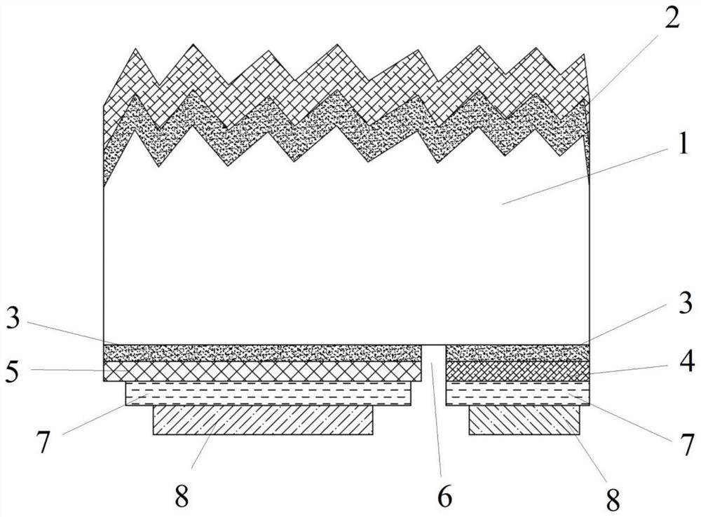
The invention provides an interdigital back contact heterojunction solar cell based on an LPCVD high-efficiency amorphous silicon doping technology. The solar cell comprises a crystalline silicon substrate, and the front surface of the crystalline silicon substrate comprises at least one passivation layer; and the back surface of the crystalline silicon substrate comprises a tunneling oxide layer,n+ doped amorphous silicon layers / p+ doped amorphous silicon layers which are alternately arranged, a laser slotting region, a passivation layer and a metal electrode from inside to outside. A cell structure combining a back contact mode and a heterojunction mode is adopted, and a doped amorphous silicon growth mode is optimized, so the passivation capability and the contact capability of the solar cell are improved under the condition that the characteristic of IBC high short-circuit current is reserved, and the manufacturing cost is effectively reduced at the same time. Through verification, the conversion efficiency of the mass production HBC cell adopting the structure provided by the invention reaches 25% or above, and is higher than the mass production conversion efficiency of the current mainstream heterojunction or TOPCon technology of 23.5%, and the open-circuit voltage reaches 710 mV or more.
Need to check novelty before this filing date? Find Prior Art

Description

Technical field

[0001] The invention relates to the technical field of solar cells, and provides a method for growing a low-cost, high-quality doped amorphous silicon passivation layer. It is especially suitable for the formation of doped amorphous silicon passivation layer in interdigital back contact heterojunction solar cells (HBC). Background technique

[0002] In recent years, the energy crisis and environmental pressure have promoted the rapid development of solar cell research and industry. At present, crystalline silicon solar cells are the most mature and widely used solar cells, accounting for more than 90% of the photovoltaic market, and will occupy a dominant position for a long time in the future. In the rapidly developing photovoltaic industry, the improvement of photoelectric conversion efficiency and the reduction of cell manufacturing costs have become the foundation of the entire photovoltaic industry. With the continuous advancement of photovoltaic cell techno...

Examples

Embodiment Construction

[0023] The technical solution of the present invention will be further described in detail below with reference to the accompanying drawings. It should be noted that the specific implementation is only a detailed description of the present invention and should not be regarded as a limitation of the present invention.

[0024] Such as figure 1 As shown, an interdigitated back-contact heterojunction solar cell based on LPCVD-based high-efficiency doped amorphous silicon technology includes a crystalline silicon substrate 1. In this embodiment, the crystalline silicon substrate 1 is an N-type Monocrystalline silicon substrate or P-type monocrystalline silicon substrate, the front surface of the crystalline silicon substrate 1 is a monocrystalline solar cell. The suede is made of conventional KOH or NaOH, and the required suede reflectivity is less than 11 % In order to get better light absorption and optimal short-circuit current. The back surface of the crystalline silicon substra...