Method for epitaxially growing GeSi quantum dots

A technology of quantum dots and epitaxy, applied in chemical instruments and methods, luminescent materials, electrical components, etc., can solve the problems of large quantum dots, difficulty in preparation, and growth of quantum dots, etc. The method is simple and practical, consistent in size and uniform in distribution Effect

Active Publication Date: 2020-10-27
INST OF PHYSICS - CHINESE ACAD OF SCI
View PDF3 Cites 2 Cited by
  • Summary
  • Abstract
  • Description
  • Claims
  • Application Information

AI Technical Summary

Problems solved by technology

[0004] However, there are certain problems in growing quantum dots on patterned substrates.
Dry etching can produce patterns with characteristic sizes of tens of nanometers, which are used to grow quantum dots of tens of nanometers. However, during the dry etching process, damage and contamination will inevitably be introduced on the growth surface; wet etching can also prepare patterns. At the same time, compared with dry etching, the surface damage can be reduced, but due to the inevitable lateral undercutting due to wet etching, it is difficult to prepare graphics with a feature size of less than 100 nanometers due to the expansion of the size of the graphics substrate. The size of the bottom-grown quantum dots is too large, and the quantum effect is not obvious

Method used


Image

  • Method for epitaxially growing GeSi quantum dots
  • Method for epitaxially growing GeSi quantum dots
  • Method for epitaxially growing GeSi quantum dots

Examples


Embodiment 1

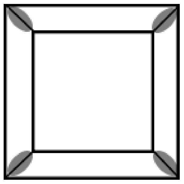
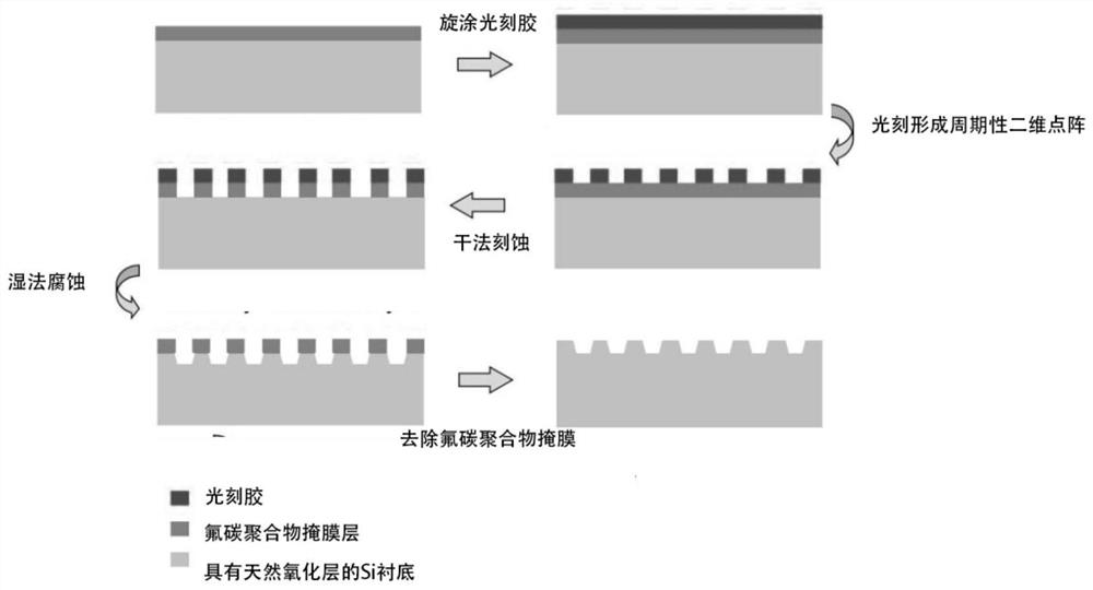
[0037] Step 1) Fabricate a truncated inverted pyramid pattern on a silicon pattern substrate.

[0038] Specific reference image 3 The flow chart of the preparation of the truncated inverted pyramid figure is shown.

[0039] First, an N-type single crystal silicon wafer with a crystal orientation of (001) is selected as a substrate, and a silicon dioxide oxide layer of 6nm to 10nm is naturally present on the surface, and a photoresist is spin-coated on it. Then, a two-dimensional photoresist lattice with a period of 600nm and a size of 240nm was prepared by an interference exposure system. Subsequently, the silicon dioxide layer was dry etched by RIE, the etching gas was CHF 3 With Ar gas, transfer the photoresist pattern to the silicon dioxide layer, and at the same time form a fluorocarbon polymer mask for subsequent wet etching. The wet etching uses KOH etching solution, the etching rate is 20nm / min, and the fluorine The carbon polymer is used as a wet etching mask to pr...

Embodiment 2

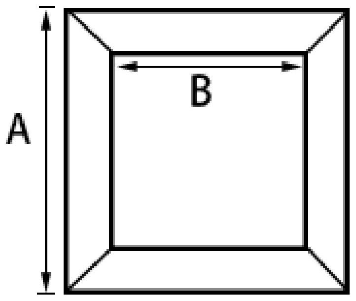
[0046] Make the truncated inverted pyramid pattern on the silicon pattern substrate, its method is the same as embodiment 1. The period of the pattern substrate is 600nm, the side length of the top opening of the pattern is 300nm, and the bottom side length is 240nm, which is a truncated inverted pyramid pattern.

[0047] The graphics substrate is placed in the gaseous source MBE, and GeSi quantum dots with a lateral size of 30nm and a height of 10nm are epitaxially grown on the truncated inverted pyramid graphics substrate, and the quantum dots are distributed on the boundary line of the (111) plane.

[0048] Gaseous source MBE was used to grow GeSi quantum dots, and disilane (Si 2 h 6 ) and germane (GeH 4 ) as the gas source of silicon and germanium respectively, control disilane flow rate to 2.5 sccm, germane flow rate to 5 sccm, and growth temperature to 600°C. Under these conditions, the growth rate of GeSi quantum dots is 0.02nm / s, and the growth time is 70s. In this ...

Embodiment 3

[0051] Make the truncated inverted pyramid pattern on the silicon pattern substrate, its method is the same as embodiment 1. The period of the pattern substrate is 600nm, the side length of the top opening of the pattern is 300nm, and the bottom side length is 140nm, which is a truncated inverted pyramid pattern.

[0052] The graphics substrate is placed in the gaseous source MBE, and GeSi quantum dots with a lateral size of 80nm and a height of 40nm are epitaxially grown on the truncated inverted pyramid graphics substrate, and the quantum dots are distributed on the boundary line of the (111) plane.

[0053] Gaseous source MBE was used to grow GeSi quantum dots, and disilane (Si 2 h 6 ) and germane (GeH 4 ) as the gas sources of silicon and germanium respectively, control the disilane flow rate to 10 sccm, the germane flow rate to 15 sccm, and the growth temperature to 600°C. Under these conditions, the growth rate of GeSi quantum dots is 0.1nm / s, and the growth time is 50...


PUM

PropertyMeasurementUnit
sizeaaaaaaaaaa
sizeaaaaaaaaaa
heightaaaaaaaaaa

Abstract

The invention provides a method for epitaxially growing GeSi quantum dots. The method comprises the following steps of: 1) preparing a truncated inverted pyramid pattern on a silicon substrate by adopting a photoetching and wet etching combined technology to obtain a patterned substrate, wherein the crystal faces of the four side faces of the truncated inverted pyramid are (111) faces; 2) removingthe mask subjected to wet etching on the patterned substrate, and cleaning the patterned substrate; 3) placing the patterned substrate in an epitaxial growth device, and directly carrying out heteroepitaxy on GeSi quantum dots on the truncated inverted pyramid patterned substrate; and 4) epitaxially growing a silicon cover layer on the GeSi quantum dots. According to the method provided by the invention, the defects that the surface of the substrate is damaged by dry etching and the feature size of grown quantum dots is too large due to the fact that the feature size of the patterned substrate prepared by wet etching is too large are avoided; and the quantum dots grown by adopting the method provided by the invention are consistent in size, and the positions of the quantum dots are highlysymmetrical, so that quadruplicated frequency of quantum dot growth is realized.

Description

technical field [0001] The invention belongs to the technical field of semiconductors. In particular, the present invention relates to methods of epitaxial GeSi quantum dots. Background technique [0002] As the most important semiconductor material at present, silicon occupies a mainstream position in the field of microelectronic device materials. With the continuous improvement of integrated circuit integration and the continuous shrinking of the size of electronic devices, the problem of RC delay is becoming more and more serious. This effect seriously restricts the ability of electronic transmission of information. In order to break through this bottleneck, a new information carrier needs to be found, and photons are the preferred object. Thanks to the development of micro-nano processing technology, silicon-based photonics has achieved a blowout development in the past ten years. At present, silicon-based optoelectronic devices have covered the fields of light emissio...

Claims


Application Information

Patent Timeline
Patent Type & Authority Applications(China)
IPC IPC(8): H01L21/203H01L21/205C09K11/66B82Y20/00B82Y40/00
CPCH01L21/02381H01L21/0243H01L21/02433H01L21/02532H01L21/02601H01L21/0262H01L21/02631C09K11/66B82Y20/00B82Y40/00
Inventor 陈弘徐然邓震贾海强王文新王森李欣欣
Owner INST OF PHYSICS - CHINESE ACAD OF SCI
Why Eureka
Try Eureka