Nickel oxide composite film, preparation method thereof and LED
A technology of composite thin film and nickel oxide, which is applied in the manufacture of semiconductor/solid-state devices, organic semiconductor devices, coatings, etc., can solve the problems of unsatisfactory hole transport effect and low work function, so as to facilitate hole transport and improve Work function, avoid complex and time-consuming preparation process
- Summary
- Abstract
- Description
- Claims
- Application Information
AI Technical Summary
Problems solved by technology
Method used
Image
Examples
preparation example Construction
[0030] On the one hand, the embodiment of the present invention provides a kind of preparation method of nickel oxide composite film, and this preparation method comprises the following steps:
[0031] S01: Provide initial nickel oxide film;
[0032] S02: depositing alkyl sulfate on the surface of the initial nickel oxide film, and then performing oxygen plasma treatment to obtain the nickel oxide composite film.
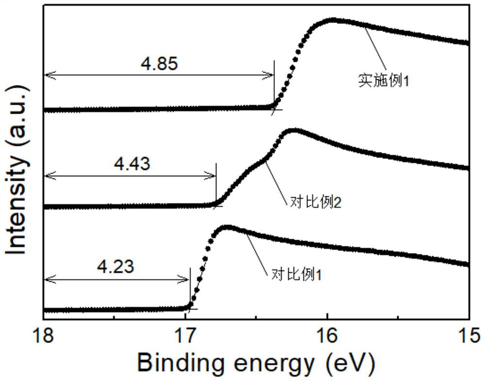
[0033] The preparation method of the nickel oxide composite film provided by the embodiment of the present invention firstly deposits an alkyl sulfate on the surface of the initial nickel oxide film, and then performs oxygen plasma treatment to obtain a modified nickel oxide composite film. The preparation method has simple process and good repeatability, and avoids the complex and time-consuming problem of the traditional metal cation doping preparation process, and the preparation method can significantly improve the work function of the nickel oxide composite fil...
Embodiment 1
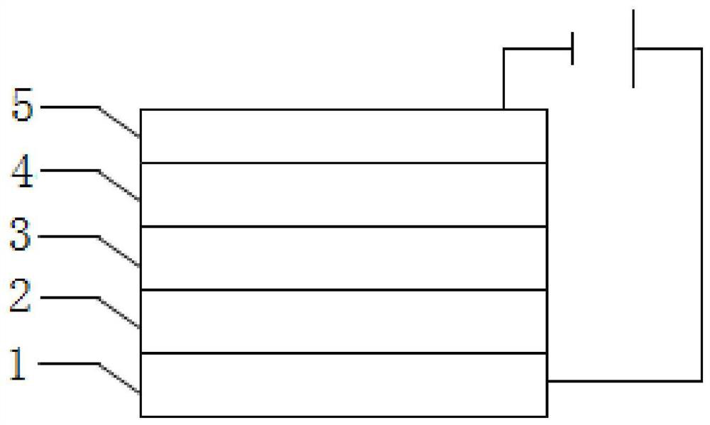
[0055] A perovskite light-emitting diode, the structure of which is as follows figure 1 As shown, it includes an anode 1 , a hole transport layer 2 , a perovskite light-emitting layer 3 , an electron transport layer 4 and a cathode 5 sequentially from bottom to top. Wherein, the material of anode 1 is ITO, the material of hole transport layer 2 is nickel oxide composite film, the material of electron transport layer 4 is TPBI, and the material of cathode 5 is LiF / Al.
[0056] The preparation steps of the above-mentioned hole transport layer 2 include:
[0057] Dissolve 1 mmol of nickel acetate tetrahydrate and 60 μL of ethanolamine in 10 ml of ethanol solution, and stir at 60 ° C for 4 hours to obtain a nickel oxide precursor solution; filter the nickel oxide precursor with a polytetrafluoroethylene filter, and place it in a 1 cm × 1 cm Spin-coat the anode ITO substrate with 50 μL of the above-mentioned nickel oxide precursor solution (prepared by solution spin-coating under ...
PUM
| Property | Measurement | Unit |
|---|---|---|
| thickness | aaaaa | aaaaa |
| electron work function | aaaaa | aaaaa |
Abstract
Description
Claims
Application Information


