High-resolution in-situ fluid turbulence heating chip of transmission electron microscope

A technology of transmission electron microscope and heating chip, which is used in material analysis using radiation, scanning probe technology, instruments, etc. It can solve the problems of lack of nanofluids, unclear heat conduction mechanism of nanofluids, and large differences in macroscopic motion behavior.

Pending Publication Date: 2020-11-03
XIAMEN UNIV
View PDF0 Cites 3 Cited by
  • Summary
  • Abstract
  • Description
  • Claims
  • Application Information

AI Technical Summary

Problems solved by technology

However, due to the large difference between the motion behavior of fluids at the nanoscale and the macroscopic motion behavior, the in-s

Method used


Image

  • High-resolution in-situ fluid turbulence heating chip of transmission electron microscope
  • High-resolution in-situ fluid turbulence heating chip of transmission electron microscope
  • High-resolution in-situ fluid turbulence heating chip of transmission electron microscope

Examples


Embodiment 1

[0084] The invention provides a method for preparing a high-resolution in-situ fluid turbulence heating chip under a transmission electron microscope. The preparation method includes the following steps,

[0085] Upper substrate production:

[0086] S101. Prepare Si(100) wafer A with silicon nitride or silicon oxide insulating layers on both sides, the thickness of silicon nitride or silicon oxide is 20nm-200nm;

[0087] S102. Using a photolithography process, transfer the upper center window and the injection port pattern from the photolithography mask to the back of the wafer A, and then develop in a positive photoresist developer to obtain a wafer A-1;

[0088] Preferably, the photolithography process is exposed under the hard contact mode of the ultraviolet lithography machine; the developing time is 50s;

[0089] More preferably, the exposure time is 15s;

[0090] S103. Utilize the reactive ion etching process to etch the upper central window and sample injection port o...

Embodiment 2

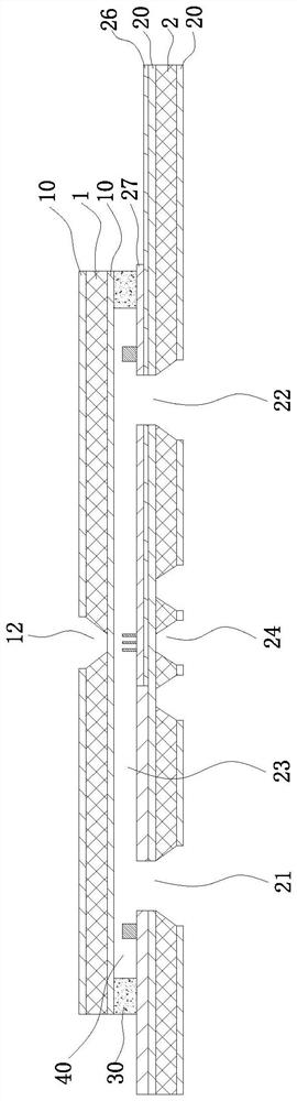
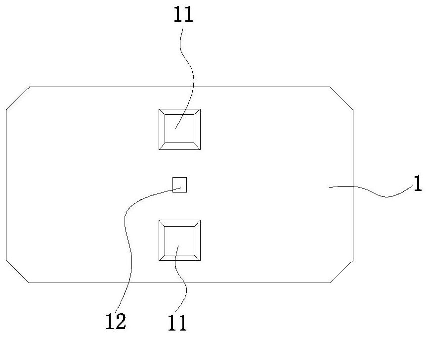
[0136] Such as Figure 1-Figure 4 As shown, the present invention provides a transmission electron microscope high-resolution in-situ fluid turbulence heating chip, the in-situ fluid turbulence heating chip includes an upper substrate 1 and a lower substrate 2, and the upper substrate 1 and the lower substrate 2 The two opposite sides are respectively defined as the front and the back; wherein, the upper substrate 1 has a first insulating layer 10 on the front and the back, and the lower substrate 2 has a second insulating layer 20 on the front and the back. In this embodiment, the materials of the upper substrate 1 and the lower substrate 2 are both silicon substrates, and the first and second insulating layers are silicon nitride or silicon oxide insulating layers.

[0137] The front side of the upper substrate 1 is bonded and fixed on the front side of the lower substrate 2 through an annular metal bonding layer 30, and an ultra-thin cavity 40 is formed by self-sealing. as...


PUM

PropertyMeasurementUnit
Thicknessaaaaaaaaaa
Thicknessaaaaaaaaaa
Thicknessaaaaaaaaaa

Abstract

The invention relates to a high-resolution in-situ fluid turbulence heating chip of a transmission electron microscope, which is structurally characterized in that an upper sheet and a lower sheet arecombined through a metal bonding layer and are self-sealed to form an ultrathin chamber; the upper piece is provided with two sample injection ports and an upper central window; the lower sheet is provided with a fluid inlet, a fluid outlet, a fluid flow channel, a lower central window, a micro-turbulence column array, a heating layer and an insulating layer; the heating layer is provided with four contact electrodes and a spiral annular heating wire; the lower central window serves as the center and is located in the central area of the spiral annular heating wire; the fluid inlet and the fluid outlet are symmetrically arranged relative to the central window, and the lower central window is located in the center of the heating layer; a micro-turbulence column array is arranged on the lower central window; the chip has the advantages of being rapid in heating and cooling, high in resolution ratio, accurate in temperature control, controllable in fluid flow direction and low in sampledrift rate.

Description

technical field [0001] The invention relates to the field of fluid chips, in particular to a high-resolution in-situ fluid turbulence heating chip for a transmission electron microscope. Background technique [0002] In situ transmission electron microscopy (TEM) is a powerful and indispensable tool for characterizing materials, providing critical structural and chemical information for them. Significant advances have been made in electron microscopy in recent years, making atomic-scale imaging a routine process. Fluid TEM has the unique advantage of being able to directly observe the transformation dynamics of materials in fluids with high spatiotemporal resolution. For example, the growth trajectory of individual nanoparticles, the electrochemical deposition and lithiation of electrode materials, and the imaging of biological materials in liquid water can be tracked. Fluid TEM can not only be used to observe the behavior of nanomaterials in a fluid environment in situ, b...

Claims


Application Information

Patent Timeline
IPC IPC(8): G01N23/04G01Q30/02G01Q30/10G01Q30/12
CPCG01N23/04G01Q30/02G01Q30/10G01Q30/12
Inventor 廖洪钢曲密江友红
Owner XIAMEN UNIV
Why Eureka
Try Eureka