Preparation method of InGaN/GaN multi-quantum well-based red light LED structure

A technology of LED structure and multiple quantum wells, which is applied in the field of microelectronics, can solve problems that are not conducive to the thermodynamic balance of In atom relaxation, high strain energy, strong quantum confinement Stark effect, etc.

Pending Publication Date: 2020-11-10
SHANDONG UNIV
View PDF0 Cites 2 Cited by
  • Summary
  • Abstract
  • Description
  • Claims
  • Application Information

AI Technical Summary

Problems solved by technology

However, this method does not adjust the energy band of the InGaN well layer, and does not stop the growth after the growth of the well layer, which will lead to a strong quantum-confined Stark effect and a high strain energy in the active region. It is beneficial for the In atoms on the surface of the well layer to relax to a suitable lattice position and reach thermodynamic equilibrium

Method used


Image

  • Preparation method of InGaN/GaN multi-quantum well-based red light LED structure
  • Preparation method of InGaN/GaN multi-quantum well-based red light LED structure
  • Preparation method of InGaN/GaN multi-quantum well-based red light LED structure

Examples


Embodiment 1

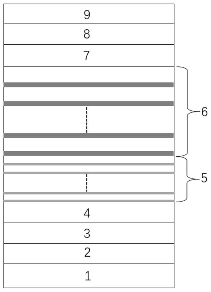
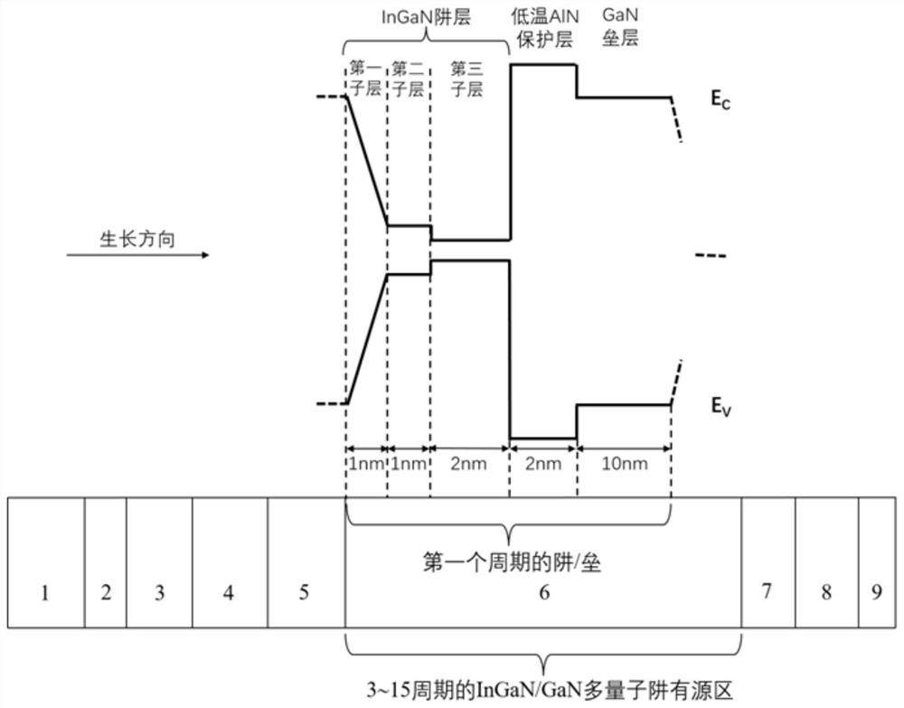
[0070] A method for preparing an InGaN / GaN multi-quantum well-based red light LED structure, such as figure 1 As shown, the InGaN / GaN multi-quantum well-based red LED structure grows sequentially from bottom to top with a sapphire substrate 1, a low-temperature GaN buffer layer 2, an undoped GaN layer 3, an n-type GaN layer 4, and an InGaN / GaN supercrystal Lattice stress release layer 5, InGaN / GaN multi-quantum well active region 6, p-type AlGaN electron blocking layer 7, p-type GaN layer 8, p-type InGaN ohmic contact layer 9, InGaN / GaN multi-quantum well active region 6 includes Several cycles of InGaN / GaN multiple quantum wells. InGaN / GaN multiple quantum wells include InGaN well layers, low-temperature AlN protective layers, and GaN barrier layers that grow sequentially from bottom to top. The first sub-layer, the second sub-layer, and the third sub-layer include the following steps:

[0071] (1) On a sapphire substrate 1 (Al 2 o 3 ) on which a low-temperature GaN buffer...

Embodiment 2

[0083] According to the preparation method of a kind of InGaN / GaN multi-quantum well-based red light LED structure described in embodiment 1, its difference is:

[0084] The following steps are performed between step A and step B: keep the temperature in the reaction chamber constant, turn off trimethylgallium (Ga source), only pass on trimethylindium (In source), and pause for 10-30s.

[0085] The method can effectively suppress In volatilization, and at the same time, allow In atoms in the well layer, especially the In atoms on the surface of the well layer, to have sufficient time to relax to a suitable lattice position and reach thermodynamic equilibrium.

Embodiment 3

[0087] According to the preparation method of a kind of InGaN / GaN multi-quantum well-based red light LED structure described in embodiment 1, its difference is:

[0088] The following steps are performed between step A and step B: keep the temperature in the reaction chamber constant, turn off trimethylgallium (Ga source), only pass on trimethylindium (In source), and pause for 25s.


PUM

PropertyMeasurementUnit
thicknessaaaaaaaaaa
thicknessaaaaaaaaaa
thicknessaaaaaaaaaa

Abstract

The invention discloses a preparation method of an InGaN / GaN multi-quantum well-based red light LED structure. The preparation method comprises the following steps: (1) sequentially growing a low-temperature GaN buffer layer, a non-doped GaN layer, an n-type GaN layer and an InGaN / GaN superlattice stress release layer on a sapphire substrate; (2) growing an InGaN / GaN multi-quantum well active region, wherein the growth process of each InGaN well layer is as follows: 1, at 680-710 DEG C, gradually increasing the flow rate of trimethyl indium from 0 to 600-700sccm, and growing a first sub-layer;2, growing a second sub-layer under the condition that the temperature and the maximum trimethyl indium flow rate in the step 1 are not changed; 3, performing cooling to 20-30 DEG C, and growing a third sub-layer; (3) sequentially growing a p-type AlGaN electronic barrier layer, a p-type GaN layer and a p-type InGaN ohmic contact layer. According to the invention, the spontaneous radiation efficiency is improved, the state density of a long-wavelength radiation area is increased, and the radiation light is expanded in the long-wavelength direction.

Description

technical field [0001] The invention relates to a method for preparing an InGaN / GaN multi-quantum well-based red light LED structure by metal organic chemical vapor deposition (MOCVD), belonging to the technical field of microelectronics. Background technique [0002] In recent years, white LEDs have been widely used in fields such as liquid crystal displays and solid-state lighting. There are three main ways to use LEDs to achieve white light emission: one is to integrate three LED chips that emit blue light, green light and red light (three primary colors) into a whole LED to emit white light; the other is to use violet LED chips as the basic light source. Violet light excites a specific phosphor to emit red, green, and blue primary colors at the same time to achieve white light emission; the third is to use the blue light emitted by the blue LED chip as the basic light source to excite the phosphor to emit yellow light, so that the blue light emitted by the LED It mixes ...

Claims


Application Information

Patent Timeline
Patent Type & Authority Applications(China)
IPC IPC(8): H01L33/12H01L33/06H01L33/32H01L33/44H01L33/00
CPCH01L33/12H01L33/06H01L33/0066H01L33/0075H01L33/44H01L33/325H01L2933/0025
Inventor 冀子武屈尚达李睿时凯居徐明升王成新徐现刚
Owner SHANDONG UNIV
Why Eureka
Try Eureka