Adhesive for high-temperature photoelectric semiconductor material and preparation method thereof

A technology of optoelectronic semiconductors and adhesives, applied in semiconductor/solid-state device manufacturing, polymer adhesive additives, non-polymer adhesive additives, etc., can solve the problem of poor control of coating thickness and uniformity, and is not suitable for repair coating Layer breakage, deposition of silicon atoms or crystals, etc., to achieve the effects of not being easily cracked or damaged, improving the uniformity and consistency of the microstructure, and improving the density

Active Publication Date: 2020-11-13
林俊贤
View PDF8 Cites 0 Cited by
  • Summary
  • Abstract
  • Description
  • Claims
  • Application Information

AI Technical Summary

Problems solved by technology

However, since the reaction between silicon vapor and solid carbon on the surface of the graphite substrate is random, the thickness and uniformity of the coating are not easy to control, and the coating needs to be re-planarized and post-treated.
Moreover, if the damaged part of the coating surface is repaired in the same way as the original method of preparing the coating, silicon atoms or crystals will also be deposited on the undamaged part, causing unnecessary waste
Therefore, there is no technical solution for repairing and reusing the coating on the surface of the stone grinding disc in the traditional technology, and the traditional method of preparing a silicon carbide coating on the surface of the stone grinding disc is not suitable for repairing the damage of the coating

Method used


Image

  • Adhesive for high-temperature photoelectric semiconductor material and preparation method thereof
  • Adhesive for high-temperature photoelectric semiconductor material and preparation method thereof

Examples


preparation example Construction

[0050] A second aspect of the present invention provides a method for preparing an adhesive for high-temperature optoelectronic semiconductor materials as described above, which includes the following steps:

[0051] (1) Take the thickener of formula quantity and add the solvent of 1 / 5 weight to stir and swell;

[0052] (2) Add filler, functional additives, polyvinyl acetate emulsion, dispersant, defoamer and remaining solvent in the stirring tank in sequence;

[0053] (3) Stir the above stirring tank, stir at 180-220 rpm for 2-5 min, then increase the stirring speed to 1200-1800 rpm, and stir for 15-30 min;

[0054] (4) Add the thickener in step (1), and stir for 10-20 minutes.
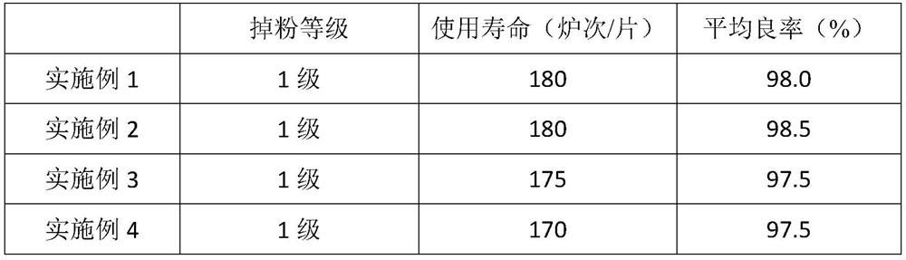
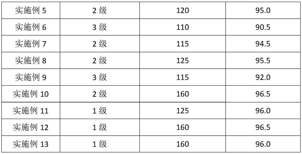
Embodiment 1

[0056] Example 1 The invention provides a kind of adhesive for high-temperature optoelectronic semiconductor material, the preparation raw material of described adhesive comprises following components: 36 parts of polyvinyl acetate emulsion, 50 parts of filler, 1.0 part of thickener, 2.0 parts of functional auxiliary agent, 0.5 part of dispersant parts, 0.4 parts of defoamer, and 10 parts of solvent.

[0057] The solvent is deionized water; the polyvinyl acetate emulsion is WX-505 of Wuhu Xingguang Synthetic Materials Co., Ltd.; the filler is a mixture of silicon powder and silicon carbide, and the weight ratio of silicon carbide and silicon powder is 1 : 4.8, the average particle diameter of described silicon powder is 30 microns, and the particle diameter of described silicon carbide is 40~50 microns, selects the green silicon carbide micropowder of Zichuan Daoxin Abrasives Factory, Zibo for use; Described thickener is hydroxyl Ethyl cellulose; the functional auxiliary agen...

Embodiment 2

[0063] Example 2 The invention provides a kind of adhesive for high-temperature optoelectronic semiconductor material, the preparation raw material of described adhesive comprises following components: 36 parts of polyvinyl acetate emulsion, 50 parts of filler, 1.0 part of thickener, 2.0 parts of functional auxiliary agent, 0.5 part of dispersant parts, 0.4 parts of defoamer, 10 parts of solvent, and 0.1 part of sodium benzoate.

[0064] The solvent is propylene glycol; the polyvinyl acetate emulsion is Shengda Chemical SD-40; the filler is a mixture of silicon carbide and silicon carbide, the weight ratio of silicon carbide and silicon powder is 1:4.8, and the silicon powder The average particle diameter of the silicon carbide is 30 microns, and the particle diameter of the silicon carbide is 40 to 50 microns, and the green silicon carbide micropowder of Zichuan Daoxin Abrasives Factory in Zibo is selected for use; the thickener is hydroxyethyl cellulose; The functional add...


PUM

PropertyMeasurementUnit
particle diameteraaaaaaaaaa
viscosityaaaaaaaaaa

Abstract

The invention relates to the technical field of semiconductor material processing, in particular to an adhesive for a high-temperature photoelectric semiconductor material and a preparation method thereof. The adhesive is prepared from the following raw materials in parts by weight: 25 to 50 parts of polyvinyl acetate emulsion, 40 to 60 parts of a filler, 0 to 1.0 part of a thickening agent, 1 to3.5 parts of a functional additive, 0.1 to 0.8 part of a dispersing agent, 0.1 to 0.8 part of a defoaming agent and 3 to 12 parts of a solvent. The adhesive has higher bonding strength on a stone milldisc; after the damaged part of the coating is brushed and repaired, the phenomenon of cracking or damage does not occur again after the coating is used for multiple times, the service life is remarkably prolonged and can be improved to 180 times per piece from 100 times per piece in the prior art, and the yield in semiconductor product production is not reduced after the coating is repaired.

Description

technical field [0001] The invention relates to the technical field of semiconductor material processing, in particular to an adhesive for high-temperature photoelectric semiconductor materials and a preparation method thereof. Background technique [0002] Semiconductor materials are necessary materials for the production of semiconductor devices and are the basis for the application of semiconductor devices. It determines and supports the level and development of the entire semiconductor electronic product. At present, the most important kind of semiconductor material is semiconductor epitaxial material, which usually includes many layers, including substrate material, buffer layer (n-type, p-type or intrinsic semiconductor material), active region, contact layer (p-type or n-type), its application range includes microelectronics, optoelectronic device circuits, such as LED, LD, PD, IC and so on. There are many methods for preparing semiconductor epitaxial materials, amon...

Claims


Application Information

Patent Timeline
Patent Type & Authority Applications(China)
IPC IPC(8): C09J131/04C09J11/08C09J11/04C09J11/06H01L21/56
CPCC08K2201/005C08L2203/206C09J11/04C09J11/06C09J11/08C09J131/04H01L21/56C08L83/12C08K13/04C08K7/26C08K3/34C08K3/36C08K5/103
Inventor 林俊贤
Owner 林俊贤
Why Eureka
Try Eureka