Optical device of flexible implantable neural photoelectrode and design and preparation method thereof

An optical device and design method technology, applied in the field of neuroscience, can solve the problems of large shear force and other stresses, difficult to achieve stable operation, low device integration and other problems, achieve long-term stable in vivo work, and reduce implantation damage. , the effect of high coupling efficiency

Active Publication Date: 2020-11-17
SHANGHAI INST OF MICROSYSTEM & INFORMATION TECH CHINESE ACAD OF SCI
View PDF7 Cites 1 Cited by
  • Summary
  • Abstract
  • Description
  • Claims
  • Application Information

AI Technical Summary

Problems solved by technology

[0004] There are also two main types of waveguide materials for implantable neural photoelectrodes. One is the optical waveguide based on polymer materials such as SU-8, but the length and width of the waveguide section generally reach 10-20 μm. It leads to larger implant size, increased implant damage, and low device integration is not conducive to the realization of high-density, multi-channel nerve cell stimulation and signal recording; another optical waveguide based on silicon nitride material, its lining The bottom of the device is made of hard material such as a silicon substrate. After the device is implanted, the Young’s modulus of the hard substrate does not match that of the brain tissue, which leads to a large shear when the device is in the body. Stress such as shear force will form a large number of nerve scars around the implant, making it difficult to achieve long-term stable work in the body

Method used


Image

  • Optical device of flexible implantable neural photoelectrode and design and preparation method thereof
  • Optical device of flexible implantable neural photoelectrode and design and preparation method thereof
  • Optical device of flexible implantable neural photoelectrode and design and preparation method thereof

Examples


Embodiment 1

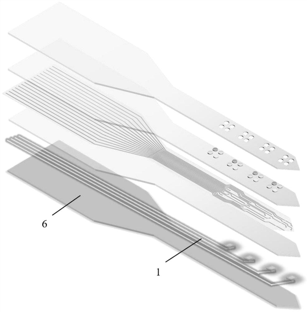
[0075] Embodiment 1 of the present invention provides an optical device of a flexible implantable neural photoelectrode, and the optical device 1 is disposed on a flexible polymer substrate 6 of the flexible implantable neural photoelectrode. The split structure of the flexible implantable neural photoelectrode is as follows: figure 1 shown. The bottom layer of the flexible implantable neural photoelectrode is an optical device 1, and the optical device 1 is arranged on a flexible polymer substrate 6, and the flexible polymer substrate 6 is made of a flexible polymer material.

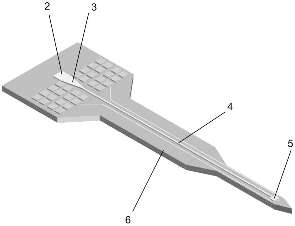
[0076] The structure of the optical device 1 of the flexible implantable nerve photoelectrode is as follows figure 2 shown. The said optical device 1 comprises:

[0077] input grating 2, waveguide 4 and output grating 5,

[0078] The input grating 2 is a parallel grating structure for coupling incident light 9 with a preset wavelength and incident angle,

[0079] The input end of the waveguide 4 ...

Embodiment 2

[0085] Embodiment 2 of the present invention provides a design method for an optical device of a flexible and flexible implantable neural photoelectrode. The optical device 1 is arranged on a flexible polymer substrate 6 of a flexible implantable neural photoelectrode. The method includes:

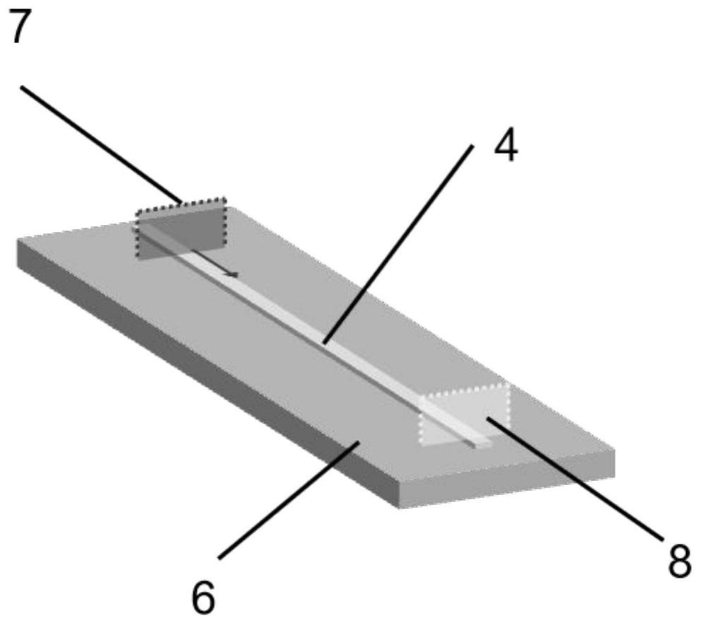
[0086] S100: Set up a mode light source 7 and a field monitor 8 on both sides of the waveguide 4, perform simulation based on the finite difference time domain method and determine the size parameters of the waveguide 4, and complete the design of the waveguide 4.

[0087] Specifically, such as image 3 and Figure 4 As shown, step S100 provided in Embodiment 2 of the present invention may include the following steps:

[0088] S110: Perform initial structure setting and parameter setting according to selected materials and process parameters, the parameter setting includes flexible polymer substrate refractive index, waveguide refractive index, waveguide size, waveguide surface roughness ...

Embodiment 3

[0125] Embodiment 3 of the present invention provides a method for preparing an optical device of a flexible implantable neural photoelectrode, such as Figure 12 As shown, the method includes:

[0126] S1: On a clean substrate, the photoresist is patterned by photolithography to obtain an alignment mark structure.

[0127] Preferably, the substrate is a single-polished silicon wafer with a thickness of 300-500 μm (for example, 400 μm), and the single-polished silicon wafer is cleaned and ready for use.

[0128] S2: Depositing metal on the patterned photoresist to obtain a metal alignment mark structure.

[0129] Specifically, on the patterned photoresist, a chromium / gold alloy layer with a thickness of 5nm / 50nm-10nm / 100nm (for example, 5nm / 100nm) is deposited by thermal evaporation, and the metal alignment is obtained by a lift-off process. markup structure.

[0130] S3: Prepare a flexible polymer substrate 6 by photolithography on the metal alignment mark structure prepar...


PUM

PropertyMeasurementUnit
thicknessaaaaaaaaaa
surface roughnessaaaaaaaaaa
thicknessaaaaaaaaaa

Abstract

The invention discloses an optical device of a flexible implantable neural photoelectrode. The optical device is arranged on a flexible polymer substrate and comprises an input grating, a waveguide and an output grating, wherein the input grating is a parallel grating and is used for coupling incident light; the input end of the waveguide is coupled with the input grating; the output end of the waveguide is coupled with the output grating; and the output grating is a focusing grating and is used for optically coupling and focusing light to irradiate above a recording electrode and providing photostimulation with single cell resolution. The invention also discloses a design and preparation method of the optical device. The optical device of the flexible implantable neural photoelectrode, provided by the invention, has the advantages that photostimulation and in-situ recording with single cell resolution are provided through design of the waveguide and the gratings; the device is small in size, so that implantation damage can be reduced, and the device is low in loss, high in coupling and strong in focusing; the high integration level of the device is beneficial to realizing multichannel and high-density nerve stimulation and recording; and by adopting the flexible polymer substrate, formation of nerve scars can be reduced, and long-term in-vivo stable work is realized.

Description

technical field [0001] The invention relates to the field of neuroscience, in particular to an optical device of a flexible implantable nerve photoelectrode and a design and preparation method thereof. Background technique [0002] The photoelectrode is an important part of the application of optogenetic tools. Its function is to introduce light into the brain to regulate neuron activity, and at the same time record the changes of neuron electrical signals under light regulation. It is an implantable neural interface device. With the in-depth application of optogenetic technology in neuroscience research and its exploration in disease treatment, photoelectrodes that cooperate with optogenetic technology have shown a lot of flowers in terms of material selection, device structure, light supply method and integration process. development trend. [0003] Among them, there are two main ways of giving light to the implanted neural photoelectrode, one is to provide light stimulat...

Claims


Application Information

Patent Timeline
Patent Type & Authority Applications(China)
IPC IPC(8): A61N5/06
CPCA61N5/0601A61N5/0613A61N2005/063
Inventor 陶虎顾驰周志涛魏晓玲
Owner SHANGHAI INST OF MICROSYSTEM & INFORMATION TECH CHINESE ACAD OF SCI
Why Eureka
Try Eureka