

Groove chip embedding process
A chip and process technology, applied in the field of groove chip embedding process, can solve the problems of reducing the area of functional parts, uneven bottom, poor reliability, etc., and achieve the effect of improving bottom interconnection and heat dissipation
- Summary
- Abstract
- Description
- Claims
- Application Information
AI Technical Summary
Problems solved by technology
Method used
Image

Examples
Embodiment 1
[0040] The groove chip embedding process provided by this embodiment includes the following steps:
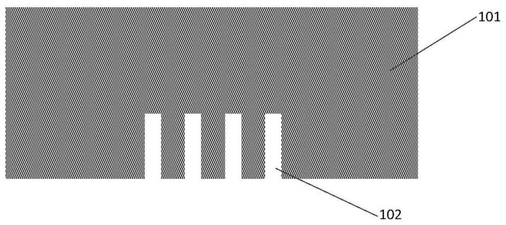
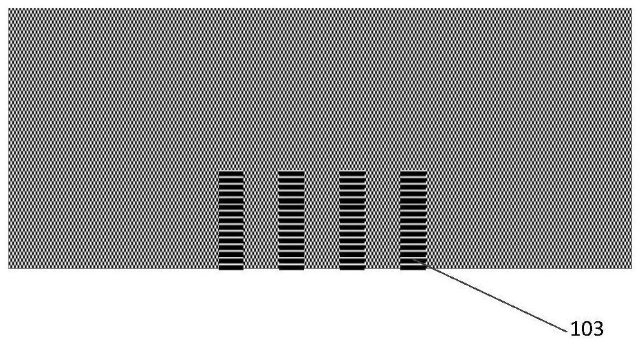
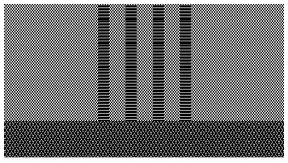
[0041] Such as figure 1 as shown,
[0042] (a), providing a silicon wafer, and etching a plurality of TSV holes on the surface of the silicon wafer to form a TSV region, then depositing a first passivation layer on the surface of the silicon wafer, and depositing at least one seed layer on the first passivation layer;
[0043] Fabricate TSV holes 102 on the surface of the base silicon wafer 101 by photolithography and etching process, the hole diameter ranges from 1um to 1000um, and the depth ranges from 10um to 1000um;
[0044] Deposit the first passivation layer such as silicon oxide or silicon nitride on the silicon wafer, or direct thermal oxidation, the thickness of the first passivation layer ranges from 10nm to 100um; by physical sputtering, magnetron sputtering or evaporation process Make a seed layer above the first passivation layer. The thickness of the seed layer ...
Embodiment 2
[0068] The groove chip embedding process provided by this embodiment includes the following steps:
[0069] Such as figure 1 as shown,
[0070] (a), providing a silicon wafer, and etching a plurality of TSV holes on the surface of the silicon wafer to form a TSV region, then depositing a first passivation layer on the surface of the silicon wafer, and depositing at least one seed layer on the first passivation layer;
[0071] Fabricate TSV holes 102 on the surface of the base silicon wafer 101 by photolithography and etching process, the hole diameter ranges from 1um to 1000um, and the depth ranges from 10um to 1000um;
[0072] Deposit the first passivation layer such as silicon oxide or silicon nitride on the silicon wafer, or direct thermal oxidation, the thickness of the first passivation layer ranges from 10nm to 100um; by physical sputtering, magnetron sputtering or evaporation process Make a seed layer above the first passivation layer. The thickness of the seed layer ...
PUM
| Property | Measurement | Unit |
|---|---|---|
| thickness | aaaaa | aaaaa |
| thickness | aaaaa | aaaaa |
| thickness | aaaaa | aaaaa |
Abstract
Description
Claims
Application Information