Preparation method of AR diffraction optical waveguide imprinting mold, soft mold and application

A diffracted light and soft mold technology, which is applied in the direction of manufacturing tools, heat treatment equipment, furnaces, etc., can solve the problems of high-efficiency and low-cost preparation of large-area tilted grating imprinting molds, high cost and complicated process steps, etc., to achieve manufacturing Low cost, low production cost, and the effect of reducing manufacturing cost

Active Publication Date: 2020-12-04
QINGDAO TECHNOLOGICAL UNIVERSITY
View PDF10 Cites 3 Cited by
  • Summary
  • Abstract
  • Description
  • Claims
  • Application Information

AI Technical Summary

Problems solved by technology

Although LIGA technology has outstanding advantages, its process steps are relatively complicated and the cost is expensive.
In order to obtain the light source, a complex and expensive high-energy X-ray source - a synchrocyclotron - is required, as well as a photolithographic mask
The photolithographic mask itself is a microstructure, which needs to be prepared by ion beam lithography and other technologies, which is time-consuming and complicated, and there are few types of photoresists available, which makes it difficult for LIGA technology to imprint large-area inclined gratings with arbitrary shapes. Efficient and low-cost preparation of molds

Method used


Image

  • Preparation method of AR diffraction optical waveguide imprinting mold, soft mold and application
  • Preparation method of AR diffraction optical waveguide imprinting mold, soft mold and application
  • Preparation method of AR diffraction optical waveguide imprinting mold, soft mold and application

Examples


Embodiment

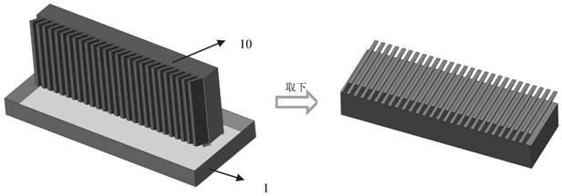
[0064] figure 1 It is a schematic diagram of an electroforming mask to be manufactured by the present invention and the specific parameters of the diffractive optical waveguide (surface relief oblique grating) that it can manufacture, wherein inclination angle, groove depth (relative depth), line width, fill factor (grating width / period) such as figure 1 mentioned. The parameters of the metal mold to be manufactured in this implementation example: the inclination angle is 35°; the groove depth is 330nm; the line width is 220nm, the period is 405nm, and the filling factor (coefficient) is 55%. A photoresist 2 is provided on the surface of the nickel plate 1 .

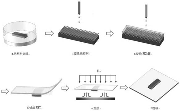
[0065] Taking the tilted grating nanoimprint mold described in the implementation example as an example, combined with Figure 1-Figure 6 , specifically explain the specific process of manufacturing tilted grating nanoimprint mold based on the proposed method and equipment.

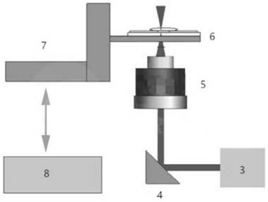
[0066] Step 1: Print the electroforming ...


PUM

PropertyMeasurementUnit
thicknessaaaaaaaaaa
thicknessaaaaaaaaaa
thicknessaaaaaaaaaa

Abstract

The invention relates to a preparation method of an AR diffraction optical waveguide imprinting mold, a soft mold and application. The preparation method comprises the specific steps that an electroforming mask is printed on a nickel substrate through a two-photon polymerization micro-nano 3D printer; nanosecond pulse micro electroforming is utilized, electroforming is conducted on the obtained nickel substrate with the mask, and an inclined grating metal nickel mold is obtained; and the manufactured inclined grating metal nickel mold serves as a female mold, the female mold is coated with a pattern layer polymer PDMS, PET is attached to the PDMS, imprinting is conducted on the mold, uncovering type demolding is adopted, the soft mold copied at a time is obtained, the steps of PDMS coating, PET attaching, imprinting and uncovering type demolding are repeated, and finally the composite soft mold with a plurality of PDMS soft mold arrays arranged on one piece of PET is prepared. High-precision, low-cost and efficient manufacturing of the large-area AR diffraction optical waveguide imprinting mold is achieved.

Description

technical field [0001] The invention belongs to the technical field of augmented reality AR and micro-nano manufacturing, and specifically relates to a method for preparing an AR diffractive optical waveguide embossing mold, a soft mold and its application. Background technique [0002] The information disclosed in this background section is only intended to increase the understanding of the general background of the present invention, and is not necessarily taken as an acknowledgment or any form of suggestion that the information constitutes the prior art already known to those skilled in the art. [0003] Augmented Reality (AR for short) is a new technology that ingeniously integrates virtual information with the real world. It can use one or a group of optical couplers to integrate the virtual information and the real scene through the "superposition" method after the virtual information simulation, and the two kinds of information complement each other, thereby realizing...

Claims


Application Information

Patent Timeline
Patent Type & Authority Applications(China)
IPC IPC(8): B29C33/38C25D1/10C22F1/10C21D9/00
CPCB29C33/3842C25D1/10C22F1/10C21D9/0068
Inventor 郭鹏飞张厚超兰红波
Owner QINGDAO TECHNOLOGICAL UNIVERSITY
Why Eureka
Try Eureka