Lightly-doped substrate, substrate with selective emitter, and solar cell and preparation method and application thereof

A lightly doped, substrate technology, applied in the field of solar cells, can solve the problems of lowering the reaction temperature, reducing the amount of carrier gas, uneven doping square resistance, etc., and achieves the effect of simple preparation method, easy realization and low price

Pending Publication Date: 2020-12-04
YANCHENG CANADIAN SOLAR INC +2
View PDF3 Cites 4 Cited by
  • Summary
  • Abstract
  • Description
  • Claims
  • Application Information

AI Technical Summary

Problems solved by technology

In the process of leading to LDSE, the doped area is prone to uneven square resistance, and the doped square resistance cannot be very low
[0004] CN107394012A discloses a silicon wafer laser-doped SE diffusion process, said process is to form a diffused first layer of phosphorus layer and a diffused second phosphorus layer on the surface of a silicon wafer, increase the deposition process of a phosphorus-attached layer and the silicon surface after diffusion Phosphorus-attached layer is formed, which not only solves the problem of insufficient PSG concentration after laser ablation, but also easily removes the phosphorous-attached layer in the subsequent phosphorus washing process, which can effectively solve the problem caused by low PSG concentration during laser doping. The problem of poor ohmic contact and low filling factor, but the energy during laser doping is high, and there is no oxide layer and buffer layer in the middle, which will lead to uneven doping resistance
And the diffusion of the second phosphorus layer may damage the doped phosphorus layer in subsequent processing, thereby affecting the uniformity of the square resistance of the doped region
[0005] CN106206847A discloses a kind of ultra-low concentration POCl based o...

Method used


Image

  • Lightly-doped substrate, substrate with selective emitter, and solar cell and preparation method and application thereof
  • Lightly-doped substrate, substrate with selective emitter, and solar cell and preparation method and application thereof

Examples


Embodiment 1

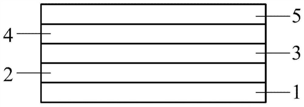
[0081] This embodiment provides a lightly doped substrate, such as figure 1 As shown, the lightly doped substrate includes a P-type silicon layer 1, an N-type silicon layer 2, a first phosphosilicate glass layer 3, an oxide layer 4 and a second phosphosilicate glass layer 5 connected in sequence, wherein the P-type silicon layer The thickness of layer 1 is 160 μm, the thickness of N-type silicon layer 2 is 0.3 μm, the thickness of the first phosphosilicate glass layer 3 is 20 nm, and the phosphorus content in the first phosphosilicate glass layer 3 is 6×10e 20 cm -3 , the thickness of the oxide layer 4 is 40nm, the thickness of the second phosphosilicate glass layer 5 is 20nm, and the phosphorus content in the second phosphosilicate glass layer 5 is 8×10e 20 cm -3 .

[0082] This embodiment also provides a method for preparing a lightly doped substrate, the preparation method comprising the following steps:

[0083] A. Entering the boat: Pre-texture the P-type silicon wafe...

Embodiment 2

[0094] This embodiment provides a lightly doped substrate, which includes a P-type silicon layer, an N-type silicon layer, a first phosphosilicate glass layer, an oxide layer, and a second phosphosilicate glass layer connected in sequence, wherein The thickness of the P-type silicon layer is 180 μm, the thickness of the N-type silicon layer is 0.1 μm, the thickness of the first phosphosilicate glass layer is 30 nm, and the content of phosphorus in the first phosphosilicate glass layer is 5×10e 20 cm -3 , the thickness of the oxide layer is 20nm, the thickness of the second phosphosilicate glass layer is 10nm, and the phosphorus content in the second phosphosilicate glass layer is 7×10e 20 cm -3 .

[0095] This embodiment also provides a method for preparing a lightly doped substrate, the preparation method comprising the following steps:

[0096] A. Entering the boat: Pre-texture the P-type silicon wafer layer to obtain the textured silicon wafer, and then put the textured ...

Embodiment 3

[0107] This embodiment provides a lightly doped substrate, which includes a P-type silicon layer, an N-type silicon layer, a first phosphosilicate glass layer, an oxide layer, and a second phosphosilicate glass layer connected in sequence, wherein The thickness of the P-type silicon layer is 140 μm, the thickness of the N-type silicon layer is 0.5 μm, the thickness of the first phosphosilicate glass layer is 10 nm, and the phosphorus content in the first phosphosilicate glass layer is 7×10e 20 cm -3 , the thickness of the oxide layer is 60nm, the thickness of the second phosphosilicate glass layer is 30nm, and the phosphorus content in the second phosphosilicate glass layer is 9×10e 20 cm -3 .

[0108] This embodiment also provides a method for preparing a lightly doped substrate, the preparation method comprising the following steps:

[0109] A. Entering the boat: Pre-texture the P-type silicon wafer layer to obtain the textured silicon wafer, and then put the textured sil...


PUM

PropertyMeasurementUnit
Thicknessaaaaaaaaaa
Thicknessaaaaaaaaaa
Thicknessaaaaaaaaaa

Abstract

The invention provides a lightly-doped substrate, a substrate with a selective emitter, and a solar cell and a preparation method and application thereof. The lightly-doped substrate comprises a P type silicon wafer layer, an N type silicon layer, a first phosphorosilicate glass layer, an oxide layer and a second phosphorosilicate glass layer which are connected in sequence. According to the invention, in the subsequent heavy doping process of the lightly-doped substrate, the doping uniformity of a doping source on the surface of a silicon wafer can be improved, and the square resistance valueof a heavy doped region can be reduced, so that the silver-silicon contact resistance is reduced; the preparation method of the lightly-doped substrate is simple, easy to implement and suitable for industrial large-scale production and application; and the phosphorus content of the heavily-doped region in the substrate with the selective emitter prepared by the lightly-doped substrate is relatively high, the sheet resistance of the heavily doped region is relatively low and uniform, and the prepared solar cell has relatively high light conversion efficiency.

Description

technical field [0001] The invention belongs to the field of solar cells, and relates to a lightly doped substrate, a substrate with a selective emitter, a solar cell and a preparation method and application thereof. Background technique [0002] Laser Doped Selective Emitter (LDSE) uses a laser beam to selectively irradiate the silicon surface to make the silicon substrate into a molten state, and the dopant atoms can quickly enter the molten silicon. When the laser beam disappears, the molten silicon After cooling and crystallization, the dopant atoms enter the silicon crystal to form a heavily doped region. [0003] Before LDSE doping, the first diffusion is carried out, and the diffused phosphosilicate glass layer is the source of LDSE doping source. At present, in order to ensure the efficiency of the battery, the square resistance of the first diffusion is relatively high, the thickness of the phosphosilicate glass layer is relatively low, and the phosphorus content i...

Claims


Application Information

Patent Timeline
IPC IPC(8): H01L31/068H01L31/0224H01L31/18
CPCH01L31/022425H01L31/068H01L31/1804Y02E10/547Y02P70/50
Inventor 刘志强袁中存费正洪
Owner YANCHENG CANADIAN SOLAR INC
Why Eureka
Try Eureka