Photoelectric detector and preparation method thereof

A photodetector and metal electrode technology, applied in the field of photoelectric detection, can solve the problems that the detection accuracy cannot be guaranteed

Active Publication Date: 2020-12-04
SOUTH CHINA NORMAL UNIVERSITY
View PDF6 Cites 4 Cited by
  • Summary
  • Abstract
  • Description
  • Claims
  • Application Information

AI Technical Summary

Problems solved by technology

Photodetectors made of zinc oxide combined with metal materials to form heterojunctions have also been widely studied, but they cannot guarantee detection accuracy, and optical filters are still required to achieve wavelength tunability

Method used


Image

  • Photoelectric detector and preparation method thereof
  • Photoelectric detector and preparation method thereof
  • Photoelectric detector and preparation method thereof

Examples


Embodiment 1

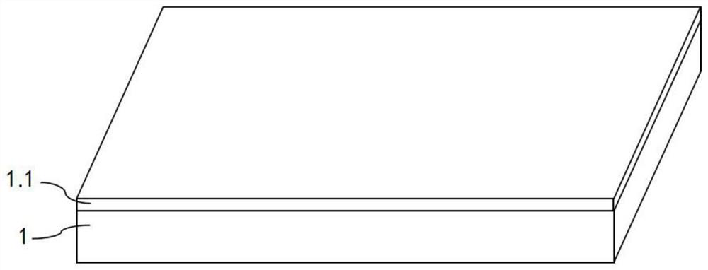
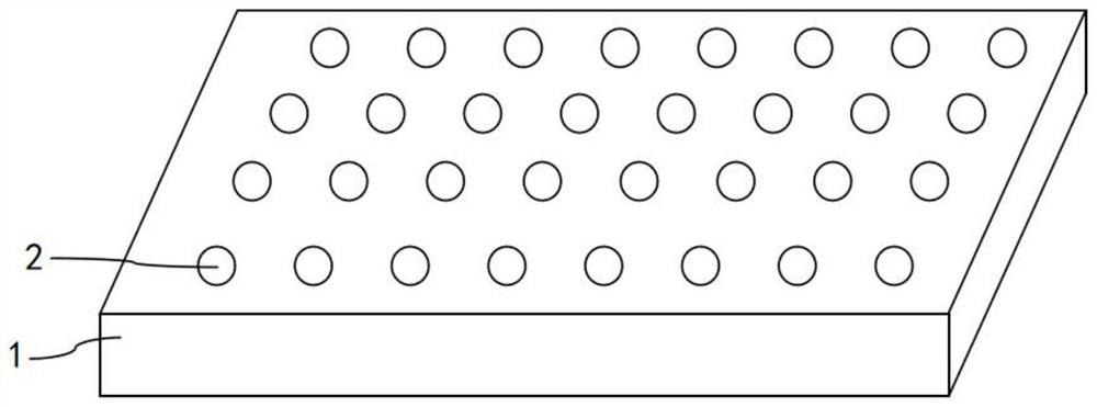
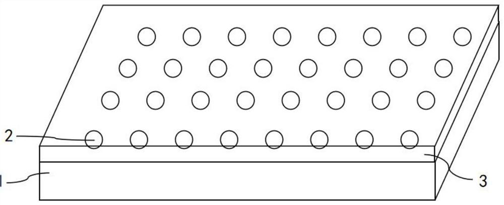
[0056] The photodetector in the present invention includes the following parts: substrate 1, metal nanoparticle layer 2, metal seed layer 3, metal nanowire array 4, insulating material 5, first metal electrode 6 and second metal electrode 7 .

[0057] Such as Figure 1-Figure 8 It is a schematic diagram of the positional relationship among the layers of the photodetector in Example 1 of the present invention during preparation. to combine Figure 1-Figure 8 , the specific preparation process of the photodetector in Embodiment 1 of the present invention is:

[0058] First, one side of the substrate 1 is polished, and a metal thin film layer 1.1 is deposited on the polished surface, and the metal thin film layer 1.1 completely covers the polished surface of the substrate 1; 1 Metal thin film layer on the polished surface 1.1 Perform rapid annealing treatment; set annealing conditions including annealing temperature, annealing time and annealing gas atmosphere.

[0059] Where...

Embodiment 2

[0068] Single-sided polished P-type silicon with a resistivity of 1-40Ω·cm, a thickness of 725μm, and a crystal orientation of is selected as the substrate 1, and the size of the substrate 1 can be adjusted arbitrarily according to requirements.

[0069] Configure NH 4 F, H 2 A mixed solution of O and HF, where NH 4 F is 40g, H 2 O is 60ml, and HF is 18ml; the silicon wafer is soaked in the prepared solution for 40-60s to remove silicon dioxide formed by oxidation on the surface of the silicon substrate 1 . After the immersion is complete, take out the silicon wafer, rinse it repeatedly with ultrapure water for 3 to 5 times, and then use air to dry the residual liquid on the surface; put the dried silicon wafer into acetone, isopropanol and ultrapure water successively Ultrasonic cleaning is performed for 5-10 minutes, and the residual liquid on the surface needs to be blown dry by air before putting in; finally, the silicon wafer is taken out and blown dry by air; the gas...


PUM

PropertyMeasurementUnit
electrical resistivityaaaaaaaaaa
thicknessaaaaaaaaaa
thicknessaaaaaaaaaa

Abstract

The invention provides a photoelectric detector and a preparation method thereof, and relates to the technical field of photoelectric detectors. The photoelectric detector comprises a substrate, a metal nanoparticle layer formed by rapid annealing a metal film layer, a metal seed crystal layer, a metal nanowire array, an insulating material, a first metal electrode and a second metal electrode. According to the photoelectric detector and the preparation method thereof provided by the invention, the metal nanoparticle layer is inserted between the metal seed crystal layer and the metal nanowirearray, so that the separation rate of photo-induced electron hole pairs in the photoelectric detector can be improved, and the illumination response speed is further improved; and by changing the material, the thickness, the annealing temperature, the annealing time and the annealing gas atmosphere of the metal film layer, the property of the metal nanoparticle layer can be changed, the absorption accuracy of the photoelectric detector on incident light is further improved, and the tunable wavelength absorption range of the incident light is realized.

Description

technical field [0001] The invention relates to the technical field of photodetection, in particular to a photodetector and a preparation method thereof. Background technique [0002] Photodetectors have been widely used in military communications, human motion sensors, Fourier transform infrared spectroscopy, medical environment monitoring, remote control, temperature sensing, thermal imaging and other fields, and have received more and more attention in recent years. Most current photodetectors are based on narrow-bandgap semiconductor materials such as indium arsenide, indium antimonide, potassium arsenide, and lead sulfide. However, this type of detector faces several challenges. First, the growth of the above-mentioned narrow-bandgap semiconductor materials is usually complicated and environmentally unfriendly, which increases the difficulty of forming heterojunctions with other materials; second, these While the narrow bandgap semiconductor material responds to light ...

Claims


Application Information

Patent Timeline
Patent Type & Authority Applications(China)
IPC IPC(8): H01L31/108H01L31/0352H01L31/18
CPCH01L31/108H01L31/0352H01L31/035227H01L31/18Y02P70/50
Inventor 王幸福朱玉
Owner SOUTH CHINA NORMAL UNIVERSITY
Why Eureka
Try Eureka