Silicon-based laminated solar cell with microstructure and preparation method thereof

A technology of solar cells and microstructures, which is applied in circuits, photovoltaic power generation, electrical components, etc., can solve the problems of low long-wavelength photon absorption efficiency and low carrier collection efficiency, so as to improve photoelectric conversion efficiency, improve charge transmission performance, and improve The effect of utilization efficiency

Active Publication Date: 2020-12-18
CHANGSHU INSTITUTE OF TECHNOLOGY +1
View PDF10 Cites 1 Cited by
  • Summary
  • Abstract
  • Description
  • Claims
  • Application Information

AI Technical Summary

Problems solved by technology

[0005] An object of the present invention is to provide a silicon-based tandem solar cell with a microstructure, which solves the problems of low long-wavelength photon

Method used


Image

  • Silicon-based laminated solar cell with microstructure and preparation method thereof
  • Silicon-based laminated solar cell with microstructure and preparation method thereof
  • Silicon-based laminated solar cell with microstructure and preparation method thereof

Examples


Embodiment 1

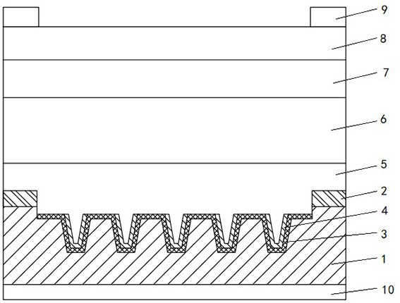
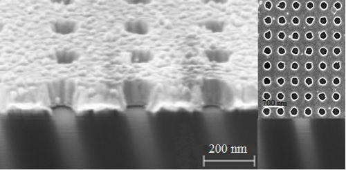
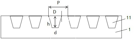
[0033] Example 1, see figure 1 , figure 2 and image 3 As shown, first, the n-type single crystal silicon substrate 1 is an n-type Czochralski single crystal silicon wafer with a size of 1 cm×1 cm, a thickness of 100 μm, and a resistivity of 1.6 Ω·cm. After cleaning, the submicron dry etching process masked by the nanoparticle self-assembled film was used to prepare an inverted nano-frustum hole 11-period array structure, using SF6 and C4F8 mixed gas, the volume flow rate was 16sccm and 18sccm, the power was 600W, and the partial The voltage is 20V, and the dry etching time is 0.3h. After forming an 11-period array of inverted nano-truncated cone holes on the surface of the silicon substrate, it was cleaned with deionized water. The period P of the formed periodic array structure of nano-frustum holes 11 is 400nm, the diameter d of the small end of the nano-frustum holes 11 is 100nm, the diameter D of the big end is 300nm, the hole depth h is 500nm, and the duty ratio is 0.7...

Embodiment 2

[0037] Example 2, please refer to Example 1. First, the n-type single crystal silicon substrate 1 is an n-type Czochralski single crystal silicon wafer with a size of 1 cm×1 cm, a thickness of 100 μm, and a resistivity of 1.6 Ω·cm. After cleaning, the submicron dry etching process masked by the nanoparticle self-assembled film was used to prepare an inverted nano-frustum hole 11-period array structure, using SF6 and C4F8 mixed gas, the volume flow rate was 16sccm and 18sccm, the power was 700W, and the partial The voltage is 30V, and the dry etching time is 0.5h. After forming an 11-period array of inverted nano-truncated cone holes on the surface of the silicon substrate, it was cleaned with deionized water. The period P of the formed periodic array structure of nano-truncated cone holes 11 is 400nm, the diameter d of the small end of the nano-truncated cone holes 11 is 100nm, the diameter D of the large end is 300nm, the hole depth h is 800nm, and the duty ratio is 0.75.

...

Embodiment 3

[0041] Example 3, please refer to Example 1. First, the n-type single crystal silicon substrate 1 is an n-type Czochralski single crystal silicon wafer with a size of 1 cm×1 cm, a thickness of 100 μm, and a resistivity of 1.6 Ω·cm. After cleaning, the submicron dry etching process masked by the nanoparticle self-assembled film was used to prepare the inverted nano-truncated cone hole 11-period array structure, using SF6 and C4F8 mixed gas, the volume flow rate was 12sccm and 22sccm, the power was 600W, and the partial The voltage is 20V, and the dry etching time is 0.3h. After forming an 11-period array of inverted nano-truncated cone holes on the surface of the silicon substrate, it was cleaned with deionized water. The period P of the formed periodic array structure of nano-frustum holes 11 is 600nm, the diameter d of the small end of the nano-frustum holes 11 is 100nm, the diameter D of the big end is 400nm, the hole depth h is 500nm, and the duty cycle is 0.66.

[0042] A...


PUM

PropertyMeasurementUnit
Diameteraaaaaaaaaa
Depthaaaaaaaaaa
Thicknessaaaaaaaaaa

Abstract

The invention provides a silicon-based laminated solar cell with a microstructure. The silicon-based laminated solar cell comprises a bottom cell structure and a top cell structure laminated on the bottom cell structure, the bottom cell structure comprises an n-type monocrystalline silicon substrate, and the periphery of the upper surface of the n-type monocrystalline silicon substrate is equippedwith a SiO2 insulating layer. A nanometer truncated cone hole periodic array structure is prepared through middle etching, a p-type doping layer is formed, an Ag thin film reflecting layer is prepared on the inner wall of the nanometer truncated cone hole, and a metal thin film layer is arranged on the lower surface of the n-type monocrystalline silicon substrate; the top cell structure sequentially comprises a TiO2 thin film layer, a perovskite absorption layer, a hole transport layer, a transparent conductive thin film layer and a metal electrode from bottom to top. The invention further discloses a preparation method of the cell. According to the invention, the excellent light capturing capability of the nanometer truncated cone hole periodic array is utilized, and the TiO2 is used forfilling the silicon hole array to improve the collection efficiency of carriers, so that the photon absorption efficiency is improved, and the photocurrent density is also improved.

Description

technical field [0001] The invention relates to a solar cell and a preparation method thereof, in particular to a silicon-based stacked solar cell with a microstructure and a preparation method thereof. Background technique [0002] Solar energy is a renewable and clean energy, which is of great significance to the sustainable development of human beings. While solar cells directly convert light energy into electrical energy, photoelectric conversion efficiency and preparation cost are the key factors that determine its industrial application. At present, the limit efficiency of silicon-based solar cells is about 29.4%, and the preparation cost to achieve this efficiency is extremely high. A laminated battery is formed by superimposing a wide-bandgap light-absorbing material on the top layer of the silicon-based battery. While taking into account the mature technology of the silicon battery, the efficiency of the battery can be improved. The theoretical limit efficiency of ...

Claims


Application Information

Patent Timeline
IPC IPC(8): H01L25/16H01L31/0352H01L31/054H01L31/068H01L31/18H01L51/42H01L51/44H01L51/48B82Y40/00
CPCH01L25/167H01L31/068H01L31/035281H01L31/035209H01L31/0547H01L31/1804B82Y40/00H10K71/12H10K30/87H10K30/30Y02E10/52Y02E10/549Y02E10/547Y02P70/50
Inventor 况亚伟张树德郑豪魏青竹刘玉申倪志春洪学鹍张德宝
Owner CHANGSHU INSTITUTE OF TECHNOLOGY
Why Eureka
Try Eureka