

Etching solution for silicon nitride layer and method for preparing semiconductor device using the same
A technology for etching solution and silicon nitride film, which is applied in semiconductor/solid-state device manufacturing, chemical instruments and methods, electrical components, etc., and can solve the problems of reducing the etching speed of silicon oxide film, abnormalities, and bad patterns, etc.
- Summary
- Abstract
- Description
- Claims
- Application Information
AI Technical Summary
Problems solved by technology
Method used
Image

Examples
preparation example Construction
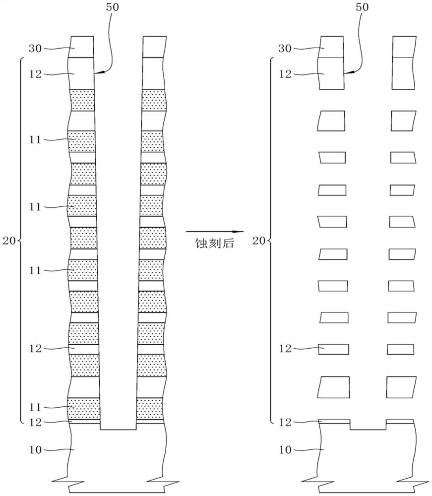
[0106] The silicon substrate used in the manufacture of semiconductor devices may contain a silicon nitride film (Si x N y ), or may contain both a silicon oxide film and a silicon nitride film (Si x N y ). Furthermore, in the case of a silicon substrate including both a silicon oxide film and a silicon nitride film, the silicon substrate may be in a form in which the silicon oxide film and the silicon nitride film are alternately stacked or stacked in different regions.
[0107] The manufacturing method of a semiconductor device according to the present invention is applicable to the manufacturing process of a computer flash memory device (NAND) device. More specifically, in the process step required to selectively remove the silicon oxide film without loss of the silicon nitride film in a stacked structure for forming a computer flash memory device, it can be performed by using the above-mentioned etching solution.
[0108] As an example, figure 1 It is a schematic cros...
Embodiment
[0114] Preparation of etching solution
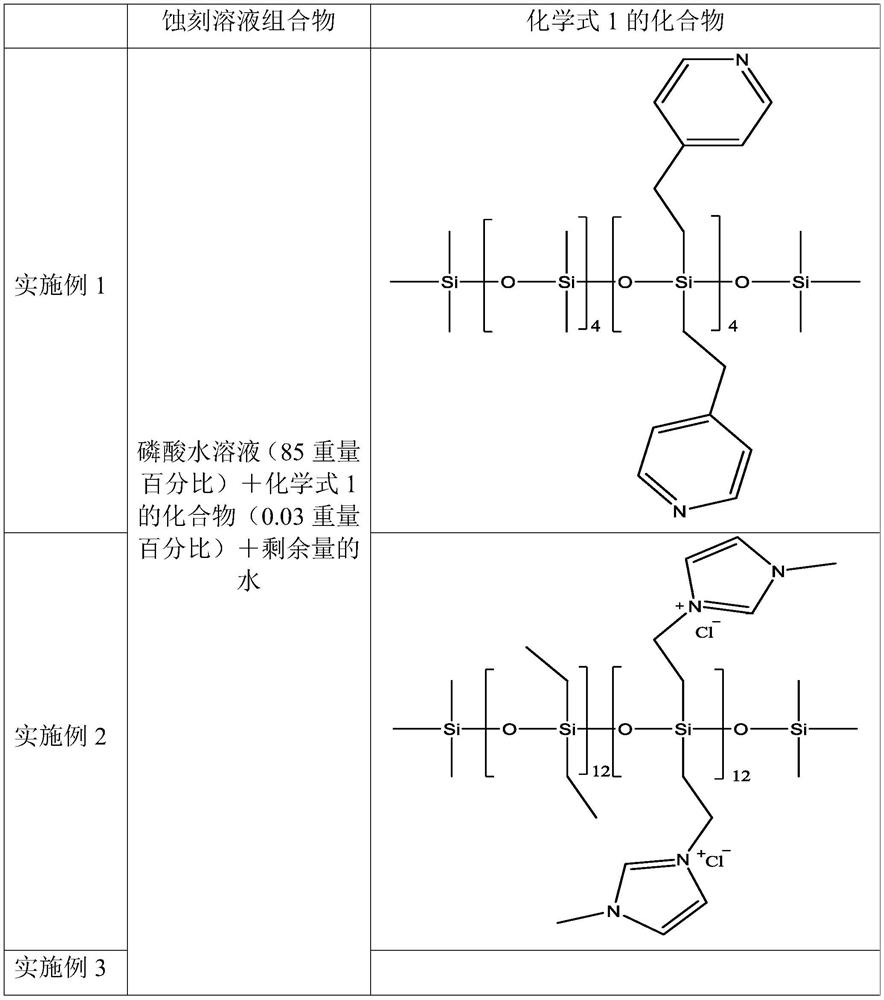
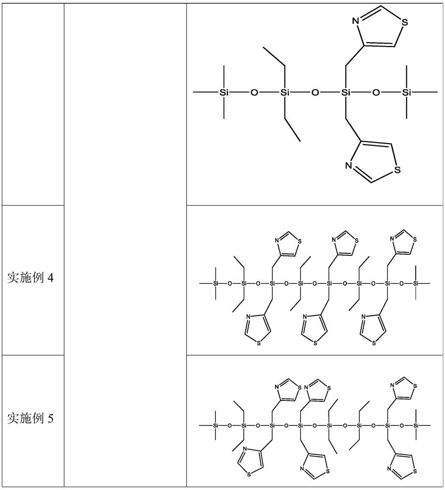
[0115] In Examples 1 to 6, the compound represented by Chemical Formula 1 was added to the phosphoric acid aqueous solution to etch the solution so that the initial concentration was 300 ppm.
[0116] The etching solution compositions according to Examples 1 to 6 and Comparative Examples 1 to 3 are shown in Table 1.
[0117] Table 1
[0118]
[0119]
[0120]
experiment example
[0122] At a temperature of 175°C, for the silicon nitride film etching solution having a combination of various examples and comparative examples, a thickness of The thermal oxide layer and the silicon nitride film were immersed in a heated etching solution and etched for 10 minutes.
[0123] Use spectroscopic ellipsometry (nano-scale Nano-View, SE MG-1000 type; Ellipsometery) to measure the thickness of silicon oxide film and silicon nitride film before etching and after etching, and the etching rate is by before etching and after etching silicon oxide film and The value calculated by dividing the thickness difference of the silicon nitride film by the time (10 minutes).
[0124] The measured etching rates are shown in Table 2 below.
[0125] Table 2
[0126]
[0127] As shown in the above Table 2, compared with the silicon nitride film etching solutions of Comparative Examples 1 to 3, the silicon nitride film etching solutions of Examples 1 to 6 can reduce the etching ...
PUM
 Abstract
Description
Claims
Application Information