Superconducting nanowire single-photon detector
A single-photon detector, superconducting nanowire technology, applied in nanotechnology, nanotechnology, nanotechnology for materials and surface science, etc., can solve the problem that fractal SNSPDs are difficult to achieve internal quantum efficiency, limit the detection efficiency of fractal SNSPDs, SNSPD absorption efficiency reduction and other problems, to achieve the effect of weakening the current crowding effect, improving the internal quantum efficiency, optimizing the internal quantum efficiency and absorption efficiency
- Summary
- Abstract
- Description
- Claims
- Application Information
AI Technical Summary
Problems solved by technology
Method used
Image
Examples
Embodiment 1
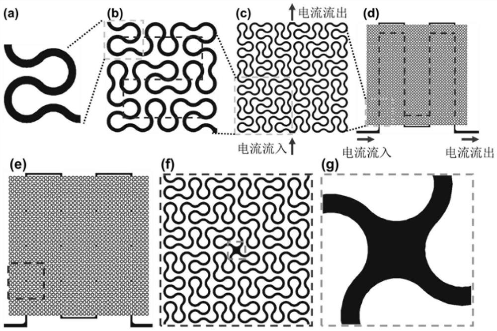
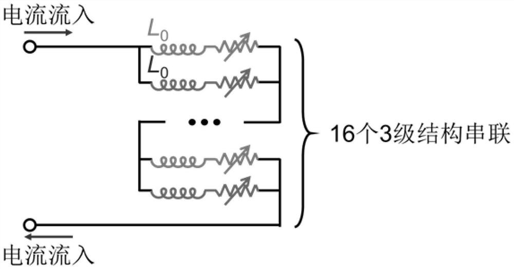
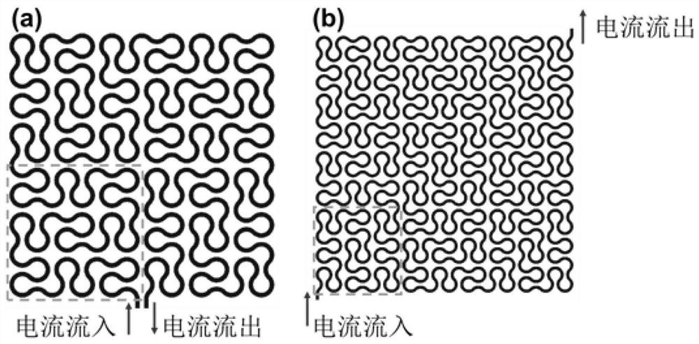
[0038] A superconducting nanowire single photon detector, see Figure 1-Figure 5 , the embodiment of the present invention designs the SNSPD as a curved fractal nanowire structure, which is used to alleviate the current crowding effect, improve the internal quantum efficiency and realize the polarization insensitivity of the detection efficiency; on the other hand, further weaken the The current crowding effect, while designing the optical structure and optimizing the absorption efficiency for the curved fractal nanowire with optimized duty cycle, realizes the simultaneous optimization of the absorption efficiency and internal quantum efficiency of the curved fractal SNSPD.
[0039] Specifically, the technical solution can be divided into two parts: (1) design and simulation of curved fractal nanowire structure; (2) design and simulation of optical cavity structure.
[0040] (1) Design and simulation of curved fractal nanowire structure
[0041] The curved fractal nanowires c...
Embodiment 2
[0055] The scheme in embodiment 1 is further introduced below in conjunction with specific examples, see the following description for details:
[0056] 1. Device processing
[0057] Here, taking the normal incidence mirror DBR cavity and the curved fractal nanowire with a line width of 40 nanometers as an example, firstly, using the ion beam assisted sputtering technology, 6 pairs of 264nm / 181nm thick bismuth nanowires with a thickness of 264nm / 181nm were sequentially sputtered on a silicon substrate. Silicon oxide (SiO 2 ) / tantalum pentoxide (Ta 2 o 5 ) layer to realize the preparation of the lower distributed Bragg reflector. Defect layer 2 is processed by ion beam assisted sputtering technology, and the material is SiO 2 . After preparing a titanium niobium nitride film on the defect layer 2 by magnetron sputtering, a gold electrode is prepared by photolithography, magnetron sputtering or electron beam evaporation, followed by scanning electron beam exposure and react...
PUM
| Property | Measurement | Unit |
|---|---|---|
| Thickness | aaaaa | aaaaa |
Abstract
Description
Claims
Application Information


