

PERC double-sided solar cell and manufacturing method thereof
A technology of solar cells and manufacturing methods, which is applied in the field of solar cells, can solve the problems of increasing the manufacturing cost of silicon wafers, and cannot fundamentally eliminate black spots and black spots, so as to increase the reflectivity, avoid the reduction of parallel resistance, and improve the conversion rate. efficiency effect
- Summary
- Abstract
- Description
- Claims
- Application Information
AI Technical Summary
Problems solved by technology
Method used
Image

Examples
no. 1 example
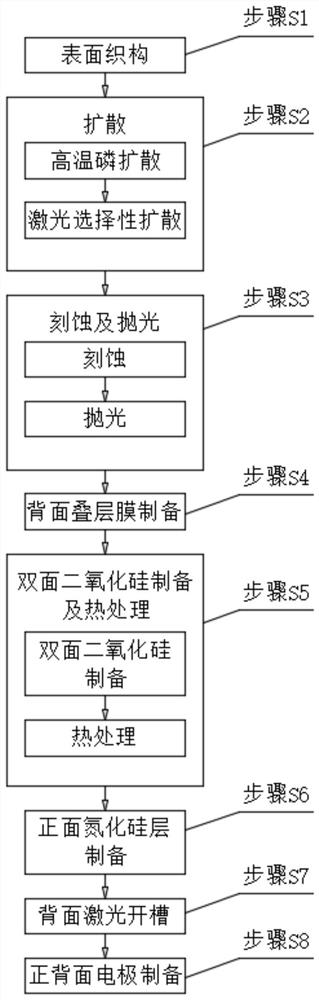
[0080] Step S1: Surface Texturing. Texture cleaning machine for surface texturing of P-type silicon wafers.
[0081] In step S1, the P-type silicon wafer is immersed in a sodium hydroxide solution with a concentration of 1.1 wt % and a temperature of 70° C., and the surface of the P-type silicon wafer is corroded into several cone-shaped surface features. P-type silicon chip response time: 220s, P-type silicon chip reflectivity: 11%.
[0082] Step S2: Diffusion. The diffusion process consists of two diffusions.
[0083] High-temperature phosphorus diffusion: Nitrogen drives phosphorus oxychloride to be charged into the diffusion furnace, and oxygen is charged into the diffusion furnace.
[0084] Laser selective diffusion: Selective diffusion and irradiation of the front electrode area of the silicon wafer by a high-energy laser. Selective diffusion rear resistance: 70Ω.
[0085] In the high-temperature phosphorus diffusion in step S2, in the high-temperature diffusion s...
no. 2 example
[0102] Step S1: Surface Texturing. Texture cleaning machine for surface texturing of P-type silicon wafers.
[0103] In step S1, the P-type silicon wafer is immersed in a sodium hydroxide solution with a concentration of 1.4 wt % and a temperature of 85° C., and the surface of the P-type silicon wafer is corroded into several cone-shaped surface features. P-type silicon chip response time: 380s, P-type silicon chip reflectivity: 12%.
[0104] Step S2: Diffusion. The diffusion process consists of two diffusions.
[0105]High-temperature phosphorus diffusion: Nitrogen drives phosphorus oxychloride to be charged into the diffusion furnace, and oxygen is charged into the diffusion furnace.
[0106] Laser selective diffusion: Selective diffusion and irradiation of the front electrode area of the silicon wafer by a high-energy laser. Selective diffusion rear resistance: 80Ω.
[0107] In the high-temperature phosphorus diffusion in step S2, in the high-temperature diffusion st...
PUM
| Property | Measurement | Unit |
|---|---|---|
| Thickness | aaaaa | aaaaa |
| Thickness | aaaaa | aaaaa |
| Diameter | aaaaa | aaaaa |
Abstract
Description
Claims
Application Information