Photoresist, patterning method of photoresist and method for generating printed circuit board
A photoresist and patterning technology, applied in the field of photoresist, can solve the problems of low resolution of photolithography pattern and high degree of roughness of line edge, and achieve the effects of improving dispersibility, improving solubility difference and improving quality
- Summary
- Abstract
- Description
- Claims
- Application Information
AI Technical Summary
Problems solved by technology
Method used
Image

Examples
Embodiment 1
[0067] Crystal Synthesis:
[0068] Ti 2 Zr 4 o 4 (OMc) 16 : 1.901g of tetrabutyl titanate, 2.681g of 80% n-butanol solution of zirconium n-butoxide and 4.095g of methacrylic acid were mixed, sealed at room temperature, and crystal Ti was obtained after a certain period of time 4 Zr 4 o 6 (OBu) 4 (OMc) 16 . 0.5gTi 4 Zr 4 o 6 (OBu) 4 (OMc) 16 Dissolve in dichloromethane, add 0.088g acetylacetone, stir for 30 minutes, remove volatile matter, the crude product is Ti 2 Zr 4 o 4 (OMc) 16 and Ti(OBu) 2 (acac) 2 The mixture, the crude product was dissolved in dichloromethane, crystallized and separated to obtain Ti 2 Zr 4 o 4 (OMc) 16 .
[0069] 0.5g metal oxide nanoparticles Ti 2 Zr 4 o 4 (OMc) 12 And 0.05g of photoacid generator N-hydroxynaphthalimide trifluoromethanesulfonic acid was dissolved in 9.45g of solvent propylene glycol monomethyl ether acetate, and filtered with a filter head with a pore size of 0.22 μm. An appropriate amount of the filtered p...
Embodiment 2
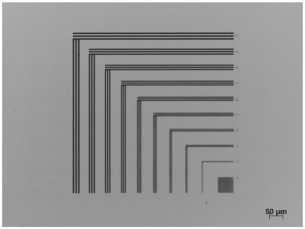
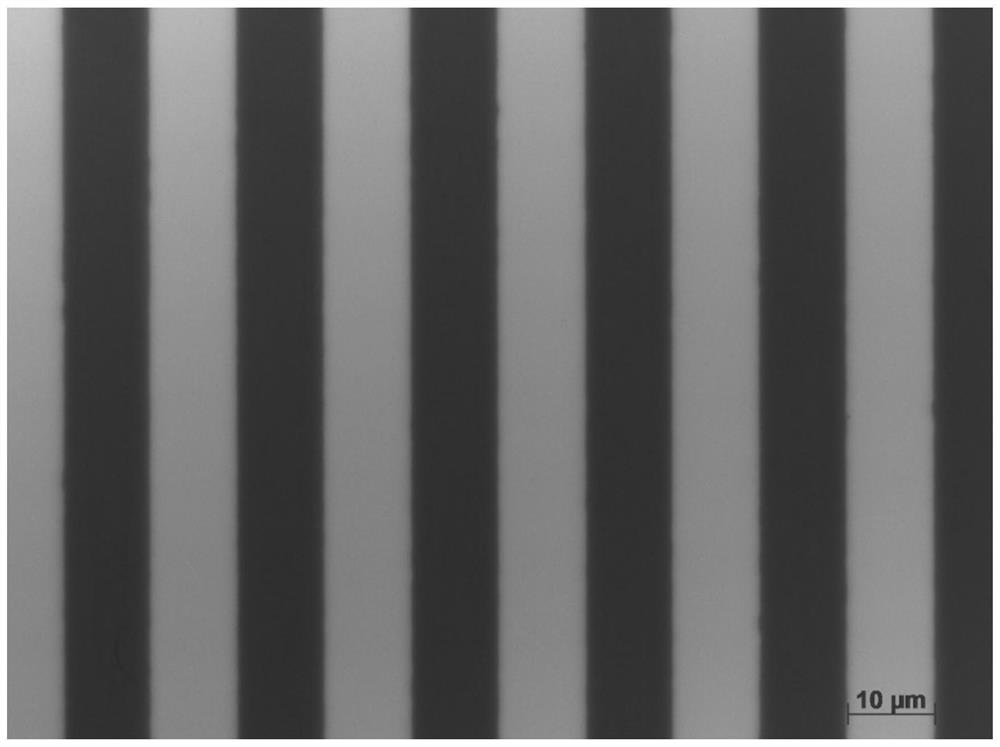
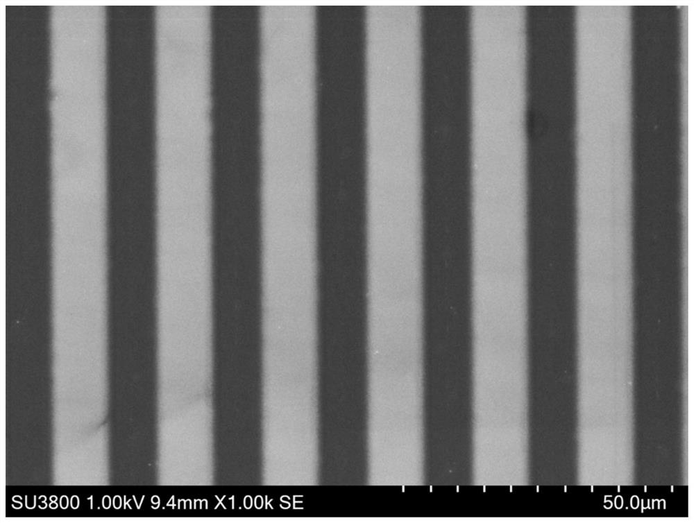
[0071] 0.5g metal oxide nanoparticles Ti 2 Zr 4 o 4 (OMc) 12 with Ti(OBu) 2 (acac) 2 The mixture and 0.05g photoacid generator N-hydroxynaphthalimide trifluoromethanesulfonic acid were dissolved in 9.45g solvent propylene glycol monomethyl ether acetate, and filtered with a filter head with a pore size of 0.22 μm. An appropriate amount of the filtered photoresist solution was dropped on the surface of the silicon wafer, and the glue was uniformed at a speed of 2000r / min for 1 minute. Dry the solvent at 100°C for 1 minute. Expose with a low-pressure mercury lamp with a wavelength of 254nm, and the exposure dose is 20mJ / cm 2 , developed with toluene, dried the surface of the silicon wafer with nitrogen, and observed the photolithographic pattern with a scanning electron microscope. The imaging pattern under the optical microscope of this embodiment is as image 3 shown.
Embodiment 3
[0072] Embodiment 3: the composition of photoresist: 5g titanium zirconium oxide nanoparticles Ti 3 Zr 5 o 3 (DMAA) 22 , 0.05g photoacid generator N-hydroxynaphthalimide trifluoromethanesulfonic acid, 4.45g solvent dichloromethane. The developer is selected from para-toluene, ortho-xylene and meta-xylene mixtures.
PUM
| Property | Measurement | Unit |
|---|---|---|
| thickness | aaaaa | aaaaa |
| thickness | aaaaa | aaaaa |
Abstract
Description
Claims
Application Information