

An Oxide Light Emitting Field Effect Transistor
A field-effect transistor and oxide semiconductor technology, applied in the field of oxide light-emitting field-effect transistors, can solve the problem that the light-emitting effect of light-emitting field-effect transistors is not very ideal, and achieve good optical transmittance, low process temperature, and good electrical performance. Effect
- Summary
- Abstract
- Description
- Claims
- Application Information
AI Technical Summary
Problems solved by technology
Method used
Image

Examples
Embodiment 1
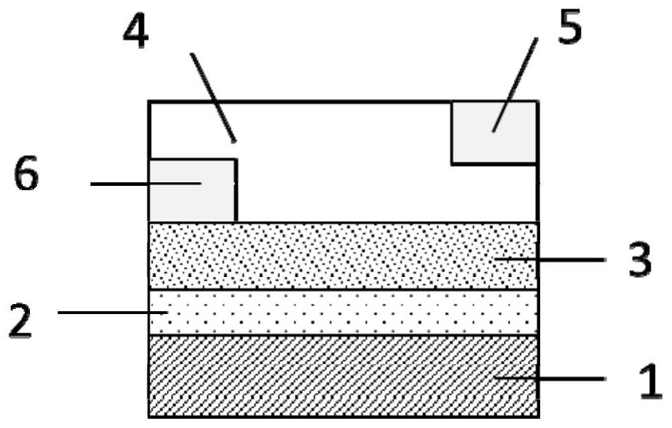
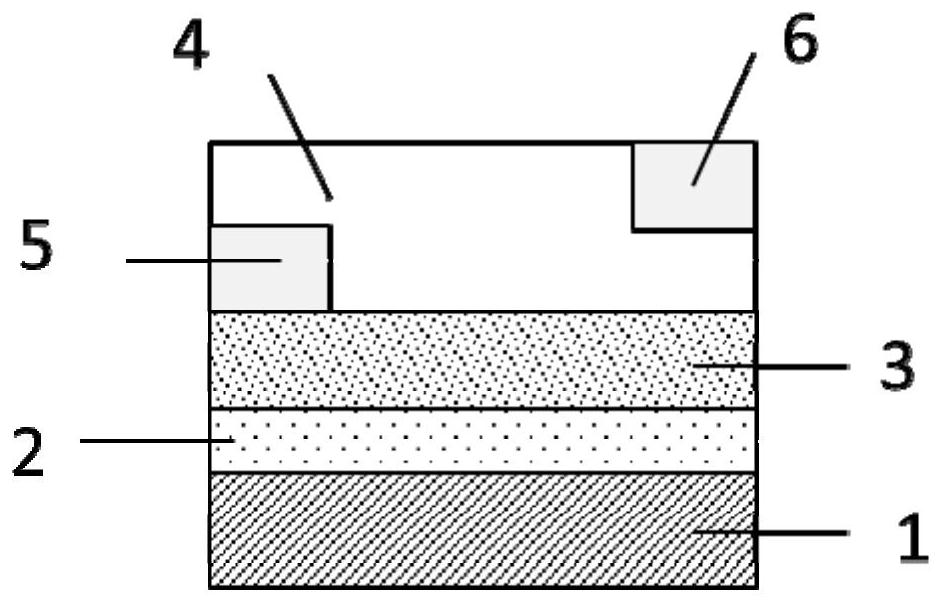
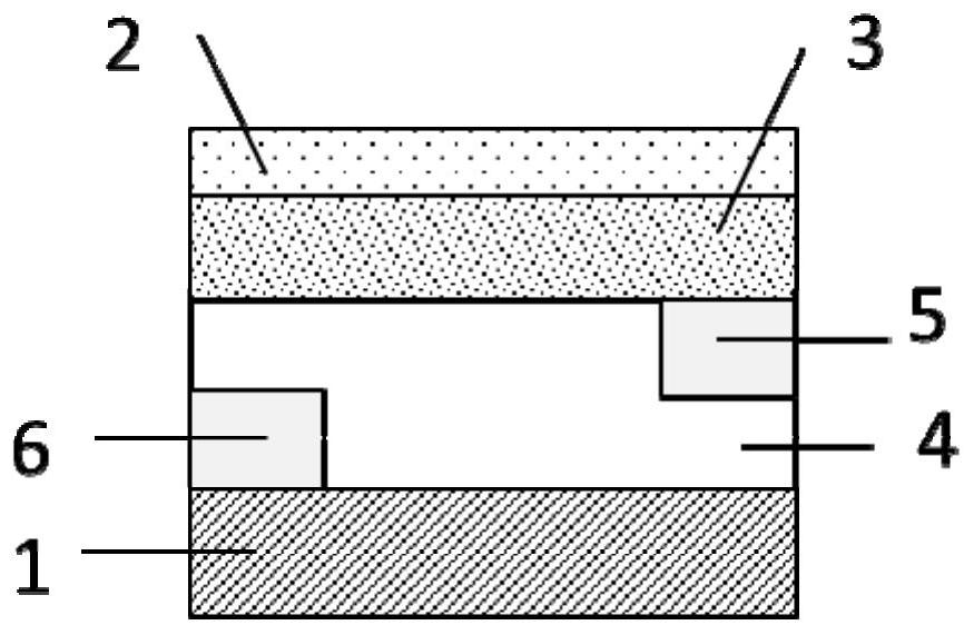
[0034] An oxide light-emitting field effect transistor is provided with a substrate, a gate, an insulating layer, an active layer, a source electrode and a drain electrode, and the oxide semiconductor material doped with rare earth elements is used as the active layer. Wherein the thickness of the active layer is 5nm-600nm.
[0035] The rare earth element in the present invention is at least one of Ce, Pr, Nd, Pm, Sm, Eu, Gd, Tb, Dy, Ho, Er, Tm or Yb. Moreover, the content of the rare earth element in the active layer is 0.2%-60% in mole percentage.
[0036] The oxide semiconductor material of the present invention is at least one of zinc oxide, indium oxide, gallium oxide, tin oxide or titanium oxide.
[0037] The structure that can be obtained in the present invention is Figure 1 to Figure 5 Light emitting field effect transistor structure. in figure 1 with figure 2 The source electrode and the drain electrode are respectively in contact with the top of the active lay...
Embodiment 2
[0041] An oxide light-emitting field effect transistor, other features are the same as those of Embodiment 1, and also has the following features: the preparation method of the active layer 4 is a vacuum method, and the heat treatment temperature of the active layer 4 is above 500°C.
[0042] It should be noted that the rare earth-doped oxide thin film can be crystallized only when the heat treatment temperature of the active layer 4 is above 500° C., so as to excite the characteristic luminescence originating from the rare earth ions.
[0043] A specific preparation method of the active layer 4 is to use a rare earth-doped oxide semiconductor material ceramic target to perform radio frequency sputtering on the surface of the insulating layer 3 to prepare a patterned active layer 4 . Wherein the power of radio frequency sputtering is 60W-200W, and the substrate temperature during deposition is 100°C-200°C.
[0044] Wherein, the preparation method of the drain electrode 6 is to...
Embodiment 3
[0051]An oxide light-emitting field effect transistor, other features are the same as those of Embodiment 1, and also has the following features: the preparation method of the active layer 4 of the present invention is a solution method, and the heat treatment temperature of the active layer 4 is 50°C-1200°C.
[0052] The specific preparation method of the active layer 4 is to perform oxygen plasma treatment on the surface of the insulating layer 3, and then spin-coat the rare earth element-doped oxide nanocrystalline material prepared by the sol-gel solvothermal method on the surface of the insulating layer 3, Then heat treatment is performed under an oxygen atmosphere to obtain the active layer 4 .
[0053] The oxide light emitting field effect transistor of the present invention can realize electroluminescence in ultraviolet, visible and infrared regions when gate voltage and drain voltage are applied.
PUM
| Property | Measurement | Unit |
|---|---|---|
| thickness | aaaaa | aaaaa |
| thickness | aaaaa | aaaaa |
| thickness | aaaaa | aaaaa |
Abstract
Description
Claims
Application Information