Cutting method for LED wafer with ITO and aluminum electrode growing on surface

A technology of surface growth and cutting method, applied in circuits, electrical components, semiconductor devices, etc., can solve the problems of limited improvement in cutting quality, internal damage to the wafer, hidden dangers of increasing cutting quality, etc., to reduce the difficulty of high-pressure cleaning and improve electrical conductivity. performance, the effect of avoiding electrochemical corrosion

Active Publication Date: 2021-03-23
SHANDONG INSPUR HUAGUANG OPTOELECTRONICS
View PDF5 Cites 0 Cited by
  • Summary
  • Abstract
  • Description
  • Claims
  • Application Information

AI Technical Summary

Problems solved by technology

However, the usual method of prefabricating the aisle is to perform corrosion or dry etching. The summation of the production process of these two methods will cause internal damage to the wafer itself, which has virtually increased the hidden danger of cutting quality. According to the method of the invention, the cutting operation, The actual cutting quality improvement is relatively limited

Method used


Image

  • Cutting method for LED wafer with ITO and aluminum electrode growing on surface
  • Cutting method for LED wafer with ITO and aluminum electrode growing on surface
  • Cutting method for LED wafer with ITO and aluminum electrode growing on surface

Examples


Embodiment 1

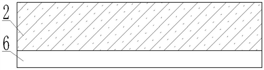
[0060] S1: Growth of epitaxial layer 2: Prepare the growth materials for epitaxial layer 2, and check the operation of each device; then take GaAs substrate 6, and grow epitaxial buffer layer, N-type gallium arsenide layer, MQW quantum A well layer, a P-type AlGaInP layer, a P-type GaAs layer, and a GaP window layer to obtain a wafer with an epitaxial layer 2;

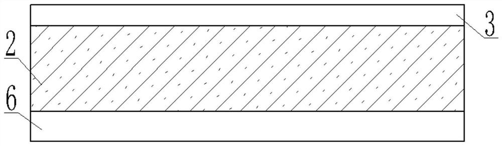
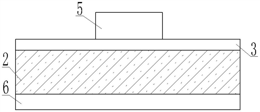
[0061] S2: grow the ITO film layer 3, and then prepare the P-face electrode structure 5: take the wafer with the epitaxial layer 2, grow the ITO film layer 3 on the surface of the epitaxial layer 2, and the ITO film layer 3 covers the entire surface of the epitaxial layer 2, wherein the ITO The thickness of the film layer 3 is The growth temperature is 270°C; and then a photoresist mask pattern is made on the surface of the ITO film layer 3 to grow the P-face electrode structure 5;

[0062] S3: Prepare N-face electrode 1: take the wafer with P-face electrode structure 5, thin the GaAs substrate 6 of the wafer, and gr...

Embodiment 2

[0068] S1: Growth of epitaxial layer 2: Prepare the growth materials for epitaxial layer 2, and check the operation of each device; then take GaAs substrate 6, and grow epitaxial buffer layer, N-type gallium arsenide layer, MQW quantum A well layer, a P-type AlGaInP layer, a P-type GaAs layer, and a GaP window layer to obtain a wafer with an epitaxial layer 2;

[0069] S2: grow the ITO film layer 3, and then prepare the P-face electrode structure 5: take the wafer with the epitaxial layer 2, grow the ITO film layer 3 on the surface of the epitaxial layer 2, and the ITO film layer 3 covers the entire surface of the epitaxial layer 2, wherein the ITO The thickness of the film layer 3 is The growth temperature is 300°C; and then a photoresist mask pattern is made on the surface of the ITO film layer 3 to grow the P-side electrode structure 5;

[0070] S3: Prepare N-face electrode 1: take the wafer with P-face electrode structure 5, thin the GaAs substrate 6 of the wafer, and gr...

Embodiment 3

[0076] S1: Growth of epitaxial layer 2: Prepare the growth materials for epitaxial layer 2, and check the operation of each device; then take GaAs substrate 6, and grow epitaxial buffer layer, N-type gallium arsenide layer, MQW quantum A well layer, a P-type AlGaInP layer, a P-type GaAs layer, and a GaP window layer to obtain a wafer with an epitaxial layer 2;

[0077] S2: grow the ITO film layer 3, and then prepare the P-face electrode structure 5: take the wafer with the epitaxial layer 2, grow the ITO film layer 3 on the surface of the epitaxial layer 2, and the ITO film layer 3 covers the entire surface of the epitaxial layer 2, wherein the ITO The thickness of the film layer 3 is The growth temperature is 330°C; and then a photoresist mask pattern is made on the surface of the ITO film layer 3 to grow the P-face electrode structure 5;

[0078] S3: Prepare N-face electrode 1: take the wafer with P-face electrode structure 5, thin the GaAs substrate 6 of the wafer, and gr...


PUM


Abstract

The invention discloses a cutting method for an LED wafer with ITO and aluminum electrodes grown on the surface. When the method is executed, the growth of an epitaxial layer is carried out, the growth of the epitaxial layer belongs to a conventional technology; an ITO film layer is grown on a GaP window layer after the epitaxial layer is grown, and therefore, the light-emitting brightness of an LED chip can be effectively improved, and the conductivity of the chip can be improved; and after the growth of the ITO film layer is finished, a P-surface electrode and an N-surface electrode are manufactured; saw blade cutting is performed by using a saw blade machine; a protective layer is grown on the P surface before cutting is performed; the chip is cleaned after cutting is performed; the residual protective layer on the surface of the wafer is removed; drying is performed, and film expansion is carried out, and therefore, an independent die structure can be formed. According to the method provided by the technical schemes is reasonable in process design and simple in operation; a cesium chloride film is used as a protective layer; and when subsequent saw blade cutting is carried out,the protective layer can effectively achieve the effects of electrode protection and cutting protection, and therefore, edge breakage and corner breakage damage are avoided to a great extent, and thewafer yield is improved.

Description

technical field [0001] The invention relates to the technical field of semiconductor processing, in particular to an LED wafer cutting method for growing ITO and aluminum electrodes on the surface. Background technique [0002] A light-emitting diode, referred to as LED (Light Emitting Diode), is a solid-state electroluminescent (EL) semiconductor device that converts electrical energy into light energy. The substantial core structure of the LED is a P-N section composed of III-IV or III-V compound materials in the element spectrum. The spectral distribution of LED light radiation has its own unique side. It is not a monochromatic light (such as a laser), nor a broad-spectrum radiation (such as an incandescent lamp), but somewhere in between, with a bandwidth of tens of nanometers and a peak wavelength in the visible or near-infrared region. Compared with ordinary light sources, LED has the following advantages: 1. High efficiency: high luminous efficiency, LED lamps and i...

Claims


Application Information

Patent Timeline
Patent Type & Authority Applications(China)
IPC IPC(8): H01L33/42H01L33/06H01L33/30H01L33/00H01L21/48
CPCH01L33/42H01L33/06H01L33/30H01L33/0062H01L21/4842
Inventor 徐晓强张兆喜王梦雪闫宝华任忠祥
Owner SHANDONG INSPUR HUAGUANG OPTOELECTRONICS
Why Eureka
Try Eureka