
Method for manufacturing semiconductor device

A semiconductor and device technology, which is applied in the field of producing miniaturized complementary semiconductor devices, can solve problems such as difficult control, increase in junction capacitance, and accelerated diffusion, and achieve the effects of suppressing increase in junction capacitance, high driving force, and suppression of short-channel effects Effect

Inactive Publication Date: 2003-10-29
PANASONIC CORP
View PDF6 Cites 0 Cited by
  • Summary
  • Abstract
  • Description
  • Claims
  • Application Information

AI Technical Summary

Problems solved by technology

As a result, the junction capacitance between the source-drain region and the substrate increases, which becomes a serious obstacle to achieve higher performance MOSFETs
Furthermore, although indium has a small diffusion coefficient, indium suffers from accelerated diffusion caused by point defects in a similar manner to boron
Moreover, indium ions are not easily activated, and compared with boron, indium ions are not easily controlled during the implantation step.

Method used


Image

  • Method for manufacturing semiconductor device
  • Method for manufacturing semiconductor device
  • Method for manufacturing semiconductor device

Examples


Embodiment 1

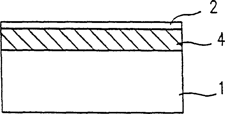
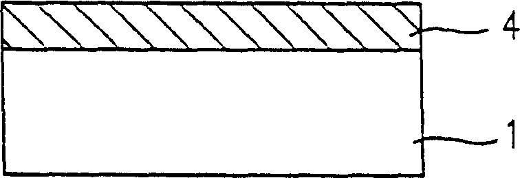
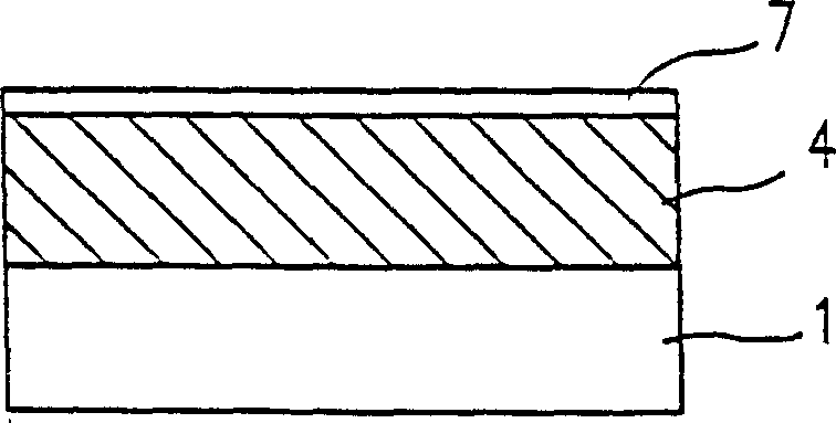
[0083] Figures 7A to 7I is a cross-sectional view showing each process step in the method for producing a semiconductor device according to the first embodiment of the present invention.

[0084] first as Figure 7A As shown, a p-type low-concentration substrate 1 is thermally oxidized to form a protective oxide film 2 for ion implantation. In the figure, reference numeral 50 denotes an insulating isolation region for device isolation.

[0085] Next as Figure 7B As shown, a mask 51 is selectively formed on the protective oxide film 2, and using the mask 51, an accelerating voltage of 400keV and 4.4×10 12 cm -2 A dose of boron is implanted, thereby forming a retrograde p-type well 3 . Also using the same mask 51, with an accelerating voltage of 160keV and 6.0×10 12 cm -2 The dose implanted boron for the formation of the channel stop layer, and with the accelerating voltage of 30keV and 4.7×10 12 cm -2 A dose of boron is implanted for forming the impurity diffusion la...

Embodiment 2

[0092] Figures 8A to 8I is a cross-sectional view showing each process step in the method for producing a semiconductor device according to the second embodiment of the present invention.

[0093] first as Figure 8A As shown, a p-type low-concentration substrate 1 is thermally oxidized to form a protective oxide film 2 for ion implantation. In the figure, reference numeral 50 denotes an insulating isolation region for device isolation.

[0094] Next as Figure 8B As shown, a mask 61 is selectively formed on the protective oxide film 2, and using the mask 61, an accelerating voltage of 400keV and 1.0×10 13 cm -2 Phosphorus is implanted at a dose of , thereby forming a retrograde n-type well 5 . Also using the same mask 61, with an accelerating voltage of 160keV and a 6.0×10 12 cm -2 The dose implanted phosphorus for forming punch-through stop layer, and with the accelerating voltage of 70keV and 6.6×10 12 cm -2 The dose implantation is used to form the BF of the impu...

Embodiment 3

[0102] Figures 9A to 9I is a sectional view showing each process step in the method for producing a semiconductor device according to the third embodiment of the present invention.

[0103] first as Figure 9A As shown, a p-type low-concentration substrate 1 is thermally oxidized to form a protective oxide film 2 for ion implantation. In the figure, reference numeral 50 denotes an insulating isolation region for device isolation.

[0104] Next as Figure 9B As shown, a mask 61 is selectively formed on the protective oxide film 2, and using the mask 61, an accelerating voltage of 400keV and 1.0×10 13 cm -2 Phosphorus is implanted at a dose of , thereby forming a retrograde n-type well 5 . Also using the same mask 61, with an accelerating voltage of 160keV and a 6.0×10 12 cm -2 The dose implanted phosphorus for forming punch-through stop layer, and with the accelerating voltage of 70keV and 6.6×10 12 cm -2 The dose implantation is used to form the BF of the impurity di...


PUM


Abstract

A method of producing a semiconductor device, comprising the steps of: forming an impurity diffusion layer for controlling a threshold voltage by ion implantation; and performing high-temperature rapid heat treatment for recovering crystal defects generated by the ion implantation. More specifically, the treatment conditions of the high-temperature rapid heat treatment are set in such a way that even if the interstitial atoms causing crystal defects diffuse, the impurities in the impurity diffusion layer do not diffuse. For example, high temperature rapid thermal processing is performed at a temperature in the range of about 900°C to about 1100°C.

Description

technical field [0001] The present invention relates to a method of producing semiconductor devices, in particular to a method of producing miniaturized complementary semiconductor devices. Background technique [0002] In Very Large Scale Integration (VLSI), there is a demand for realizing CMOS technology capable of stably realizing high-performance transistor characteristics. However, with the miniaturization of devices, the reduction of the temperature at which the production process is performed, etc., a large number of point defects are generated in the semiconductor substrate during the ion implantation step, such as the high-energy ion implantation performed when forming wells and buried layers, That is, vacancies and interstitial atoms (such as interstitial silicon) may cause accelerated diffusion of channel impurities used to control threshold voltage, which may adversely affect the redistribution of impurities in subsequent thermal treatment steps. More specifical...

Claims


Application Information

Patent Timeline
Patent Type & Authority Patents(China)
IPC IPC(8): H01L21/265H01L21/28H01L21/324H01L21/74H01L21/8238H01L29/10
CPCH01L21/2652H01L21/28185H01L21/28211H01L21/324H01L21/74H01L21/823807H01L21/823892H01L29/105H01L21/2658H01L21/8238
Inventor 赤松克立小田中绅二海本博之
Owner PANASONIC CORP
Learn More