Preparation method of multilayer electronic product
A technology for electronic products and insulating layers, which is applied in the field of preparation of multilayer electronic products, can solve the problems of incapable of industrial application, inability to achieve integration, and low production efficiency, so as to facilitate industrial application, reduce the probability of accidental short circuit, and reduce the cost Effect
- Summary
- Abstract
- Description
- Claims
- Application Information
AI Technical Summary
Problems solved by technology
Method used
Image
Examples
preparation example Construction
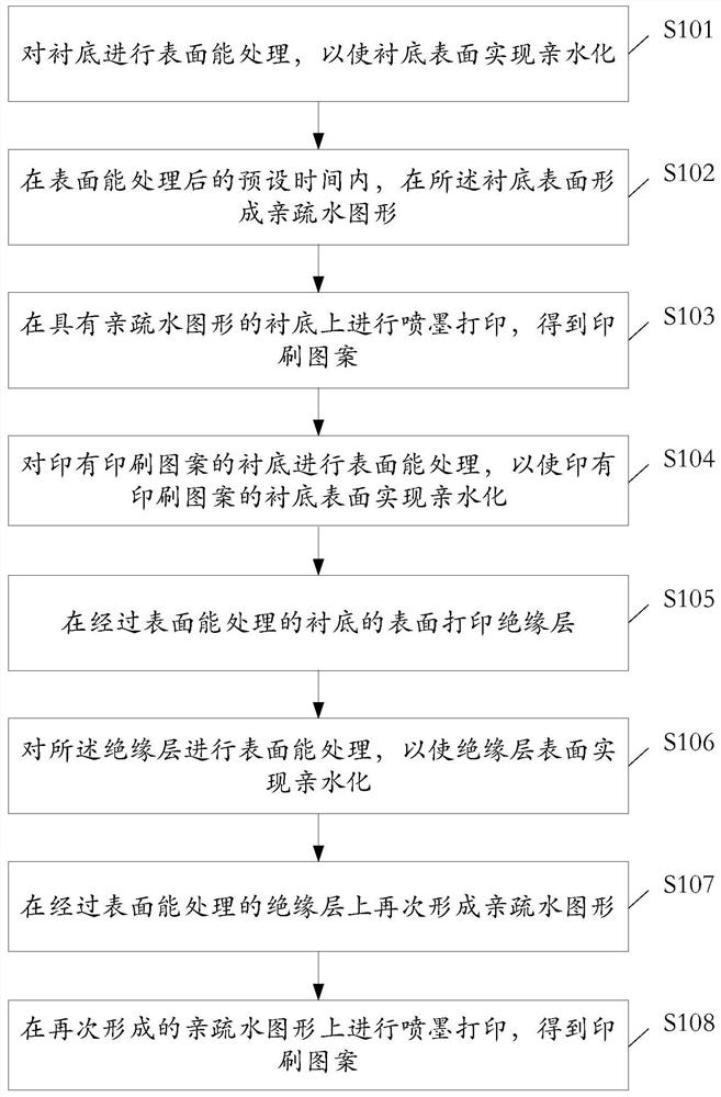
[0065] Such as figure 1 As shown, the present invention provides a kind of preparation method of multilayer electronic product, comprising:
[0066] S101, performing surface energy treatment on the substrate to make the surface of the substrate hydrophilic;
[0067] The substrate of the present invention needs to be subjected to surface energy treatment in advance, and the surface energy treatment is preferably strong oxidation treatment. The specific process includes: cleaning the substrate; drying the cleaned substrate; drying the dried substrate The substrate is subjected to strong oxidation treatment, and the strong oxidation treatment is at least one of ozone treatment, oxygen plasma treatment, and ultraviolet light treatment, so that active Si-O-(H) groups are formed on the surface of the substrate.
[0068] Specifically, when the strong oxidation treatment is ozone treatment, it has the advantages of simplicity, convenience, and strong versatility of equipment.
[006...
Embodiment 1
[0158] (1) select glass as the substrate, carry out strong oxidation treatment for 5-50 minutes (the preferred time is 30 minutes) to the highly active ozone component produced by the ultraviolet cleaning machine to the substrate, so that the substrate surface forms active Si- O-(H) group;
[0159] (2) Select a seal made of silicone rubber containing -O-Si-R groups, and the seal is made of polydimethylsiloxane;
[0160] (3) Within 1s after the end of the strong oxidation treatment, quickly roll the printing roller with the stamp fixed on the surface of the substrate with Si-O-(H) groups, and limit the contact pressure to about 1000Pa . The rolling speed is 50 mm / s, and the average contact time between the stamp and the surface of the substrate is approximately 1 ms based on the calculation that the width of the contact area between the printing roller and the plane is 50 microns. Changing the water contact angle of the substrate from about 15°C to about 70°C;
[0161] The s...
Embodiment 2
[0170] (1) Select glass as the substrate, and use a spray gun treated with atmospheric pressure plasma to process the substrate, with an average processing time of 3-5s, so that active Si-O-(H) groups are formed on the surface of the substrate;
[0171] (2) Select a seal made of silicone rubber containing -O-Si-R groups, and the seal is made of methyl vinyl silicone rubber;
[0172] (3) within 30s after the strong oxidation treatment, the printing roller fixed with the stamp is quickly rolled over the substrate surface with Si-O-(H) groups, and the contact pressure is limited to about 2000Pa, The rolling speed is 5 mm / s, and the average contact time between the stamp and the substrate surface is approximately 10 ms based on the 50 micron width of the contact area between the printing roller and the plane. This treatment makes the water contact angle of the substrate change from about 20°C to about 75°C;
[0173] The stamp is separated from the substrate with Si-O-(H) groups t...
PUM
| Property | Measurement | Unit |
|---|---|---|
| boiling point | aaaaa | aaaaa |
| surface tension | aaaaa | aaaaa |
| size | aaaaa | aaaaa |
Abstract
Description
Claims
Application Information


