Preparation method of thin-layer two-dimensional material

A two-dimensional material and thin-layer technology, applied in the field of two-dimensional materials, can solve the problems of limited application, difficulty in obtaining few-layer or even single-layer two-dimensional materials, etc., and achieve the effect of improving quality, large area and improving contact effect

Active Publication Date: 2021-05-25
SHANGHAI INST OF TECH
View PDF22 Cites 4 Cited by
  • Summary
  • Abstract
  • Description
  • Claims
  • Application Information

AI Technical Summary

Problems solved by technology

[0004] However, the traditional solvent exfoliation method is difficult to obtain few-layer or even single-layer 2D materials during practical operation, which limits its further application.

Method used


Image

  • Preparation method of thin-layer two-dimensional material
  • Preparation method of thin-layer two-dimensional material
  • Preparation method of thin-layer two-dimensional material

Examples


Embodiment 1

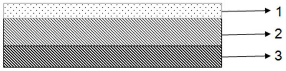
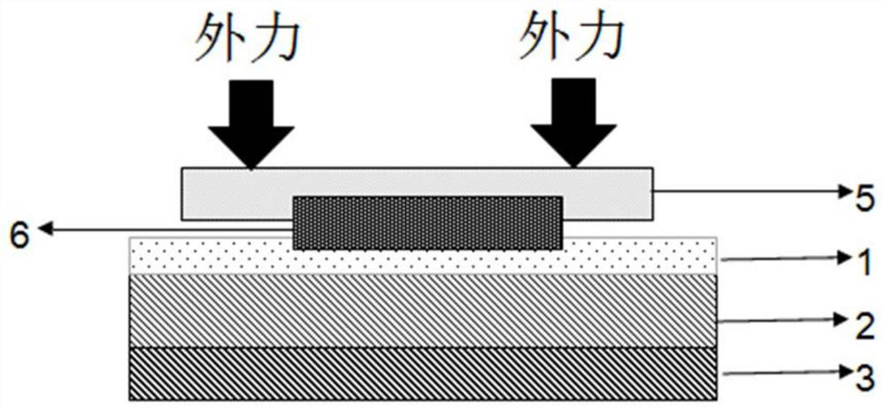
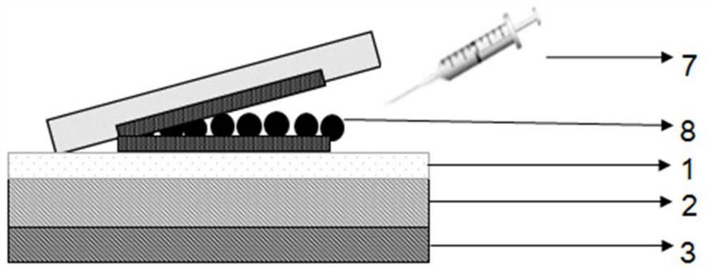
[0044] Such as figure 1 , figure 2 , image 3 Shown, the preparation method of thin-layer two-dimensional material comprises the following steps:

[0045] In the first step, the SiO 2 Dropping the first solvent on the surface of the substrate 2 to obtain the first solvent layer 1;

[0046] In the second step, use 3M-Scotch tape 5 to stick MoS 2 , and the MoS 2 Coated with tape to SiO with first solvent layer 1 2 on substrate 2;

[0047] The third step is to use the syringe 7 to extract the second solvent 8, fill the gap in the adhesive tape 5, and completely fill the adhesive tape 5 with the second solvent 8 through penetration;

[0048] In the fourth step, the above-mentioned sample is put into an oven as a whole, and heat-treated at a temperature of 66°C, and the sample is taken out of the oven after 24 hours;

[0049] In the fifth step, thermal peeling is obtained to adhere to the SiO 2 MoS on substrate 2 2 Two-dimensional materials6. Such as Figure 4 As shown...

Embodiment 2

[0052] SiO after treatment for different second solvents 8 2 MoS obtained by stripping the surface tape 2 The yield and area of ​​the lamina were counted. The statistics are divided into two items: one for MoS 2 The size is more than 0.2*10 each 5 μm 2 , 1.2*10 5 μm 2 The number of thin layers, such as Figure 8 shown; the other is the maximum size achieved by the thin layer, such as Figure 9 shown. S1-S5 in the figure represents the corresponding sample (S1-acetone; S2-isopropanol; S3-ethanol; S4-deionized water; S5-untreated) processed by different second solvents 8, and the sample selected in the experiment is in SiO 2 The substrate 2 with a layer of ethanol spin-coated on the surface can be seen from the figure, based on the process method of four solvents: acetone, isopropanol, ethanol, and deionized water, which exceeds 0.2*10 5 μm 2 The number of thin layers are 20, 31, 19, 10 respectively, more than 1.2*10 5 μm 2 The numbers of samples are 5, 13, 10, and ...

Embodiment 3

[0054] Field-effect transistors were prepared by using the two-dimensional material prepared in Example 1 and the two-dimensional material prepared by the traditional solvent stripping method, respectively. Substrate 2 is made of silicon dioxide (SiO 2 ) layer, and the insulating layer 3 adopts a silicon (Si) sheet. The electrical contact material is composed of electronic or hole-type organic semiconductors, in which the hole-type semiconductor layers are respectively made of copper phthalocyanine (CuPc), nickel phthalocyanine (NiPc), zinc phthalocyanine (ZnPc), cobalt phthalocyanine (CoPc), platinum phthalocyanine (PtPc), free phthalocyanine (H 2 Pc), Tetrathiophene (4T), Pentathiophene (5T), Hexathiophene (6T), Bis(biphenyl-4,4')-2,2'-dithiophene (BP2T) , the electronic semiconductor layer is made of fluorocopper phthalocyanine (F16CuPc), fluorophthalocyanine zinc (F16ZnPc), fluorophthalocyanine iron (F16FePc), fluorophthalocyanine cobalt (F16CoPc), chlorophthalocyanine c...


PUM

PropertyMeasurementUnit
thicknessaaaaaaaaaa

Abstract

The invention relates to a preparation method of a thin-layer two-dimensional material, which comprises the following steps: 1) dropwise adding a first solvent on a substrate to obtain a first solvent layer; 2) adhering the two-dimensional material by using an adhesive tape, and adhering the adhesive tape adhered with the two-dimensional material to the substrate containing the first solvent layer, so that the two-dimensional material is in contact with the first solvent layer; 3) injecting a second solvent below the adhesive tape; 4) performing heat treatment; and 5) stripping the adhesive tape to obtain the thin-layer two-dimensional material adhered to the substrate. Compared with the prior art, the thin-layer two-dimensional material prepared by the method has the advantages of large area, thin thickness, high yield, simple operation process, no need of large-scale film preparation equipment, and no obvious toxicity since auxiliary materials involved in the process are common solvents in laboratories. Compared with a traditional solvent stripping method, the method has the advantages that the probability of obtaining few-layer even single-layer two-dimensional materials is obviously improved, and the quality of the prepared materials is improved.

Description

technical field [0001] The invention belongs to the technical field of two-dimensional materials, and relates to a method for preparing thin-layer two-dimensional materials. Background technique [0002] The two-dimensional nanostructure material represented by graphene is an important member of the nano family and occupies a pivotal position. Compared with other nanostructures, two-dimensional nanostructures have the characteristics of large specific surface area, high surface carrier transport rate, and excellent electromechanical properties. With these advantages, this type of material has considerable application potential in many fields. , Two-dimensional nanostructures have always been one of the research focuses of researchers at home and abroad. However, so far, there are still a large number of unsolved problems in the research of two-dimensional nanostructures, no matter in various stages from material preparation, performance evaluation to final practical applica...

Claims


Application Information

Patent Timeline
Patent Type & Authority Applications(China)
IPC IPC(8): H01L21/02H01L29/24H01L29/786H01L29/80H01L51/05H01L51/42H01L51/30H01L51/46B82Y10/00B82Y30/00B82Y40/00
CPCH01L21/02568H01L29/24H01L29/78696H01L29/802B82Y10/00B82Y40/00B82Y30/00H10K10/486H10K10/484H10K30/15H10K2102/00Y02E10/549
Inventor 王军毛毓珂陈赛赛王桂东蔡金华
Owner SHANGHAI INST OF TECH
Why Eureka
Try Eureka