Optical laminating method for silicon-based OLED micro-display device
A micro-display device and silicon-based technology, which is applied in the manufacturing of semiconductor devices, electric solid-state devices, and semiconductor/solid-state devices, etc., can solve the problems of low bonding and alignment accuracy, poor bonding flatness, and complicated process flow. , to achieve the effect of saving labor costs, good contrast, and simplifying the process
- Summary
- Abstract
- Description
- Claims
- Application Information
AI Technical Summary
Problems solved by technology
Method used
Image


Examples
Embodiment 1
[0032] A silicon-based OLED microdisplay device optical bonding method, comprising the following steps:
[0033] 1) The thin-film-encapsulated silicon wafer and cover glass containing OLED and CMOS circuits are cleaned and then dried; the cover glass is cleaned with water, and the washing tank is respectively ultrasonic vibration + megasonic vibration; Wafers are rinsed with two fluids or megasonic waves; after cleaning and drying, silicon wafers and cover glass are inspected by AOI equipment, and defective products are picked out or marked.
[0034] 2) Coating the silicon wafers containing OLED and CMOS that have passed the AOI inspection with filling materials: the filling material uses OCR glue; Can achieve;
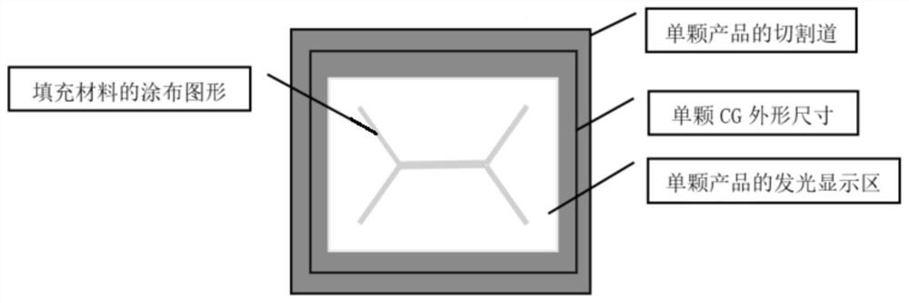
[0035] 3) Lay the glue-coated silicon wafer and the cover glass in alignment: take the silicon wafer coated with the filling material and the cover glass one by one for alignment and lamination; the size of the cover glass is one unit The size of each piece contains...
Embodiment 2
[0038] A silicon-based OLED microdisplay device optical bonding method, comprising the following steps:
[0039] 1) The thin-film-encapsulated silicon wafer and cover glass containing OLED and CMOS circuits are cleaned and then dried; the cover glass is cleaned with water, and the washing tank is respectively ultrasonic vibration + megasonic vibration; The film is washed with two fluids or megasonic wave;
[0040] 2) Use AOI equipment to inspect the cleaned and dried silicon wafers and cover glass, and pick out or mark the defective products; use the ring guide rail to carry out the follow-up process, and the first stage will go to the pick-up station 1 first. After the operation is completed, the first stage moves on the circular guide rail; first moves to the dispensing station 2, and dispenses the entire silicon wafer containing OLED and CMOS that has passed the AOI inspection; at the same time The second carrier enters the unloading station 1 to perform the unloading and ...
PUM
 Abstract
Description
Claims
Application Information
 - R&D
- Intellectual Property
- Life Sciences
- Materials
- Tech Scout
- Unparalleled Data Quality
- Higher Quality Content
- 60% Fewer Hallucinations
Browse by: Latest US Patents, China's latest patents, Technical Efficacy Thesaurus, Application Domain, Technology Topic, Popular Technical Reports.
© 2025 PatSnap. All rights reserved.Legal|Privacy policy|Modern Slavery Act Transparency Statement|Sitemap|About US| Contact US: help@patsnap.com