Preparation method of tungsten ditelluride nanobelt

A tungsten ditelluride and nanobelt technology, applied in binary selenium/tellurium compounds, nanotechnology, metal selenide/telluride, etc., can solve the problem of inability to achieve large-area production, consuming a lot of time and energy, and reducing device performance. and other problems, to achieve the effect of reducing temperature, realizing recycling and good quality

Active Publication Date: 2021-06-11
XIANGTAN UNIV
View PDF7 Cites 5 Cited by
  • Summary
  • Abstract
  • Description
  • Claims
  • Application Information

AI Technical Summary

Problems solved by technology

Although the gas-phase transport method does produce high-quality bulk crystals, the process requires prolonged annealing at high temperatures of up to 1000°C, which is time-consuming and labor-intensive
Chinese invention CN109809372A provides a method for preparing a single-layer tungsten diselenide nanoribbon, which can be prepared by atmospheric pressure chemical vapor deposition. The introduction of more impurities leads to poor product quality and reduces the performance of the device, and the small amount of product obtained on the substrate cannot achieve large-scale production

Method used


Image

  • Preparation method of tungsten ditelluride nanobelt
  • Preparation method of tungsten ditelluride nanobelt
  • Preparation method of tungsten ditelluride nanobelt

Examples


Embodiment 1

[0038] SiO to be purchased 2 / Si (300nm) substrate was sheared to obtain a substrate with a size of 1cm×1cm, which was cleaned with acetone solution, isopropanol solution, ethanol solution and deionized water in sequence, and then dried under nitrogen atmosphere. Place the treated substrate and tungsten foil as follows: first place the polished side of the silicon wafer on the graphite sheet, and then place the oxidized tungsten foil (conventional oxidation treatment: place the tungsten foil on a 5 cm outer diameter, In a clean quartz glass tube with a length of 1m, oxidize at 700°C for 60min) to cover the silicon wafer, place a gasket between the substrate and the tungsten foil, then place the graphite sheet in the center of the tube furnace, and finally put the tellurium powder The alumina porcelain boat is placed upstream of the tube furnace. The mass of the tellurium powder is 600mg, the size of the tungsten foil is 1cm x 1cm, and the distance between the tellurium powder...

Embodiment 2 to 4

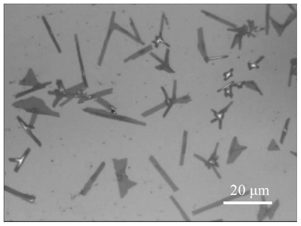
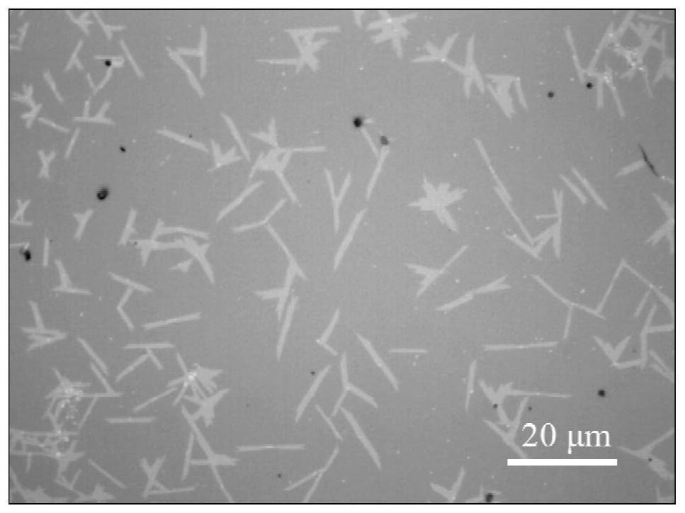
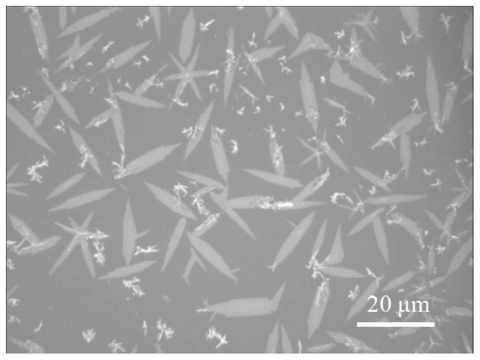
[0040] The silicon dioxide substrate in Example 1 was replaced by a sapphire substrate, a glass substrate, and a mica substrate respectively, and other preparation conditions remained unchanged, and tungsten ditelluride nanobelts with better quality could also be prepared.

[0041]The obtained tungsten ditelluride nanosheet sample is subjected to optical microscope, Raman, atomic force characterization, surface potential, scanning electron microscope characterization transmission electron microscope and XPS characterization, the results are as follows figure 1 , 2, 3, 4, 5, 6, 7, 8, 9, 10, 11, 12 and 13. It can be seen from the optical microscope characterization data that there are two-dimensional nanosheets of different layers and sizes on the silica, sapphire, and glass substrates. Taking the product obtained in Example 1 as an example, it can be seen from the Raman characterization data that the sample obtained in Example 1 is at 163 cm -1 and 212cm -1 for WTe 2 Two typ...


PUM

PropertyMeasurementUnit
thicknessaaaaaaaaaa

Abstract

The invention discloses a preparation method of a tungsten ditelluride nanobelt. The method comprises the following steps: firstly, placing a polished surface of a substrate on a graphite sheet upwards, then covering a silicon wafer with a tungsten foil subjected to oxidation treatment, and placing a gasket between the substrate and the tungsten foil so as to form a micro-reaction cavity of a sandwich-like structure. On the basis of adopting a space confinement strategy, a reaction precursor is designed at the same time, and the tungsten foil subjected to oxidation treatment is used for providing a tungsten source, so that controllable preparation of the tungsten ditelluride nanobelt is realized. By controlling the oxidation time of the tungsten foil at high temperature, the size and morphology of the tungsten ditelluride nanobelt are effectively regulated and controlled. Meanwhile, controllable growth of the tungsten ditelluride nanobelt on different substrates such as sapphire, mica and glass is realized. According to the method, controllable preparation of the large-area WTe2 nanobelt can be realized, and a new synthesis path is provided for industrial application of the WTe2 nanobelt.

Description

technical field [0001] The invention relates to a preparation method of tungsten ditelluride, in particular to a preparation method of a tungsten ditelluride nanobelt. Background technique [0002] Since the discovery of graphene materials, due to its unique physical properties, it has attracted extensive attention from researchers. A large number of studies have shown that graphene has excellent properties such as high mobility, high thermal conductivity, high strength, and high light transmittance, making it show broad application prospects in the fields of electronics, optical devices, and sensors. However, graphene is a semimetal with zero band gap, and the current switching ratio of the field effect crystal based on it is extremely low (~10), which greatly hinders its application in the semiconductor field. Therefore, researchers have been committed to exploring new graphene-like materials with semiconductor properties, such as hexagonal boron nitride, transition metal...

Claims


Application Information

Patent Timeline
Patent Type & Authority Applications(China)
IPC IPC(8): C01B19/04B82Y40/00
CPCC01B19/007B82Y40/00C01P2004/20C01P2004/02C01P2002/82C01P2004/03C01P2004/04C01P2002/85Y02E60/36
Inventor 郝国林何艳兵陈涛周国梁
Owner XIANGTAN UNIV
Why Eureka
Try Eureka