Preparation method of silicon-based CdTe-GeSn-CdTe heterogeneous transverse PiN diode and silicon-based CdTe-GeSn-CdTe heterogeneous transverse PiN diode device

A diode and silicon-based technology is applied in the field of preparation of silicon-based CdTe-GeSn-CdTe hetero-lateral PiN diodes. Integration and Stealth, Performance Improvement, Effects of Improved Microwave Characteristics

Pending Publication Date: 2021-06-18
ENG UNIV OF THE CHINESE PEOPLES ARMED POLICE FORCE
View PDF4 Cites 0 Cited by
  • Summary
  • Abstract
  • Description
  • Claims
  • Application Information

AI Technical Summary

Problems solved by technology

However, in traditional PiN diodes, the presence of intrinsic silicon or germanium materials reduces the carrier mobility and distribution uniformity; at the same time, the existence

Method used


Image

  • Preparation method of silicon-based CdTe-GeSn-CdTe heterogeneous transverse PiN diode and silicon-based CdTe-GeSn-CdTe heterogeneous transverse PiN diode device
  • Preparation method of silicon-based CdTe-GeSn-CdTe heterogeneous transverse PiN diode and silicon-based CdTe-GeSn-CdTe heterogeneous transverse PiN diode device
  • Preparation method of silicon-based CdTe-GeSn-CdTe heterogeneous transverse PiN diode and silicon-based CdTe-GeSn-CdTe heterogeneous transverse PiN diode device

Examples


Embodiment 1

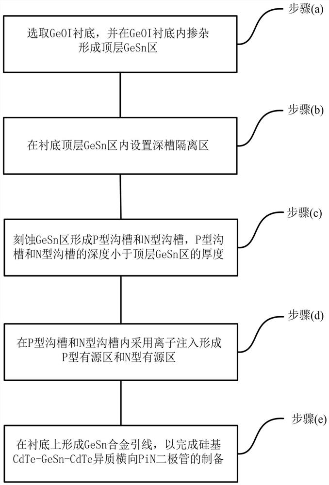
[0065] See figure 1 , figure 1 It is a flowchart of a method for fabricating a silicon-based CdTe-GeSn-CdTe heterogeneous lateral PiN diode according to an embodiment of the present invention, the method is suitable for preparing a lateral solid-state plasma PiN diode based on a GeOI substrate, and the silicon-based CdTe-GeSn-CdTe Heterogeneous lateral PiN diodes are mainly used to make silicon-based highly integrated antennas. The method comprises the steps of:

[0066] (a) select a GeOI substrate, and dope in the GeOI substrate to form a top GeSn region;

[0067] (b) setting a deep trench isolation region in the GeSn region on the top layer of the substrate;

[0068] (c) etching the GeSn region to form a P-type trench and an N-type trench, and the depth of the P-type trench and the N-type trench is less than the thickness of the top-layer GeSn region;

[0069] (d) forming a P-type active region and an N-type active region by ion implantation in the P-type trench and the ...

Embodiment 2

[0109] See Figure 2a-Figure 2t , Figure 2a-Figure 2t It is a schematic diagram of a method for preparing a silicon-based CdTe-GeSn-CdTe heterogeneous lateral PiN diode according to an embodiment of the present invention. On the basis of the first embodiment above, the length of the intrinsic region is 80 microns (the length of the intrinsic region can be in A silicon-based CdTe-GeSn-CdTe heterogeneous lateral PiN diode between 50 microns and 150 microns) is described in detail as an example, and the specific steps are as follows:

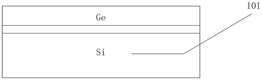
[0110] S10, selecting a GeOI substrate.

[0111] See Figure 2a , the crystal orientation of the GeOI substrate 101 may be (100) or (110) or (111), without any limitation here. In addition, the doping type of the GeOI substrate 101 can be n-type or p-type, and the doping concentration is, for example, 0.5×10 14 ~1×10 15 cm -3 , the thickness of the top layer Ge is, for example, 30-120 μm.

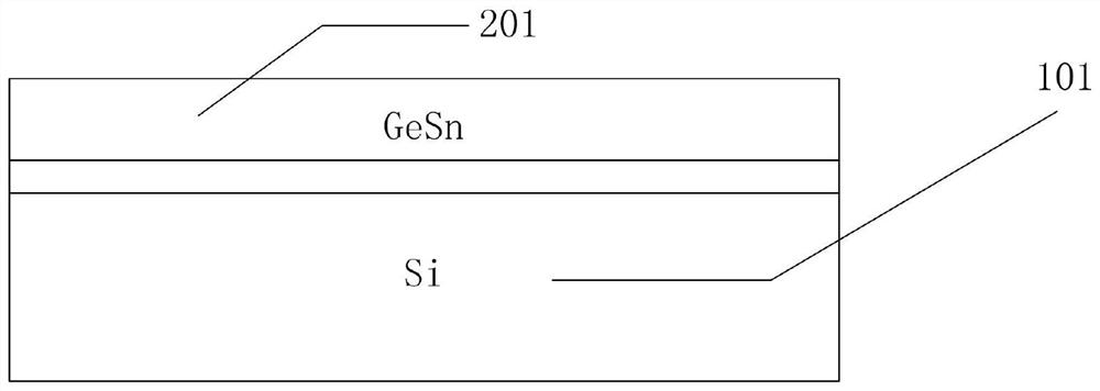
[0112] S20, doping in the GeOI substrate to form a...

Embodiment 3

[0153] Please refer to image 3 , image 3 It is a schematic diagram of the device structure of a silicon-based CdTe-GeSn-CdTe heterogeneous lateral PiN diode according to an embodiment of the present invention. The silicon-based CdTe-GeSn-CdTe heterogeneous lateral PiN diode adopts the above-mentioned figure 1 The preparation method shown is made, specifically, the silicon-based CdTe-GeSn-CdTe heterogeneous lateral PiN diode is prepared and formed on the GeOI substrate 301, and the P region 303, the N region 304 of the diode, and the lateral position of the P region 303 The intrinsic regions between the N region 304 and the N region are all located in the top GeSn layer 302 of the substrate. Wherein, the PiN diode adopts deep trench isolation technology, that is, a deep trench isolation region 307 is provided outside the P region 303 and the N region 304, and the depth of the isolation trench 307 is greater than or equal to the thickness of the top GeSn layer 302. In addit...


PUM

PropertyMeasurementUnit
Thicknessaaaaaaaaaa
Thicknessaaaaaaaaaa
Thicknessaaaaaaaaaa

Abstract

The invention relates to a preparation method of a silicon-based CdTe-GeSn-CdTe heterogeneous transverse PiN diode and a device of the silicon-based CdTe-GeSn-CdTe heterogeneous transverse PiN diode. The preparation method comprises the following steps: selecting a GeOI substrate, and doping in the GeOI substrate to form a top GeSn region; arranging a deep groove isolating region in the GeSn region on the top layer of the substrate; etching the GeSn region to form a P-type groove and an N-type groove of which the depths are smaller than the thickness of the top layer GeSn region; forming a P-type active region and an N-type active region in the P-type groove and the N-type groove by adopting ion implantation; and forming a GeSn alloy lead on the substrate, so that the preparation of the silicon-based CdTe-GeSn-CdTe heterogeneous transverse PiN diode is completed. According to the diode disclosed by the invention, the carrier mobility and the distribution uniformity are greatly improved by introducing the top GeSn region, meanwhile, the carrier transport characteristic is greatly improved, and the microwave characteristic of the solid-state plasma PiN diode is remarkably improved.

Description

technical field [0001] The invention relates to the technical field of semiconductor materials and device manufacturing, in particular to a method for preparing a silicon-based CdTe-GeSn-CdTe heterogeneous lateral PiN diode and a device thereof. Background technique [0002] With the rapid development of science and technology, the advancement of antenna technology has become an important driving force for the transformation of modern communication systems. Modern communication systems have been developing in the direction of low power consumption, broadband, and high integration. And the demand for on-board information electronics is getting higher and higher, which requires the development of flexible reconstruction technology, broadband technology and system miniaturization technology for modern antenna systems. At the same time, the radar cross section is a key performance indicator of modern antenna systems. How to effectively reduce the radar cross section of antennas ...

Claims


Application Information

Patent Timeline
IPC IPC(8): H01L29/868H01L29/06H01L21/329
CPCH01L29/868H01L29/0603H01L29/0684H01L29/6609
Inventor 苏汉王华剑
Owner ENG UNIV OF THE CHINESE PEOPLES ARMED POLICE FORCE
Why Eureka
Try Eureka