A flexible conductive metal pattern and its preparation method, application and conductive material

A conductive metal and pattern technology, which is applied in the manufacture of conductive/semiconductive layer equipment, conductive layers on insulating carriers, cable/conductor manufacturing, etc., can solve the problems of poor conductivity and damage of patterns, and achieve good flexibility, The effect of simple and time-saving process

Active Publication Date: 2022-07-12
NORTHWESTERN POLYTECHNICAL UNIV
View PDF10 Cites 0 Cited by
  • Summary
  • Abstract
  • Description
  • Claims
  • Application Information

AI Technical Summary

Problems solved by technology

In addition, the metal layer formed by printing metal precursors needs to undergo high-temperature post-treatment before it can conduct electricity, and high temperature will cause irreversible damage to plastic or paper substrates; and the formed pattern has poor conductivity due to being too thin

Method used


Image

  • A flexible conductive metal pattern and its preparation method, application and conductive material
  • A flexible conductive metal pattern and its preparation method, application and conductive material
  • A flexible conductive metal pattern and its preparation method, application and conductive material

Examples


Embodiment 1

[0045] This embodiment provides a method for preparing a flexible conductive metal pattern, which includes the following steps:

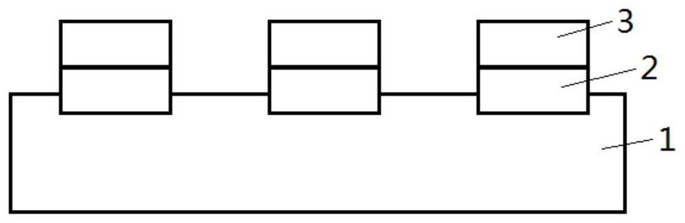
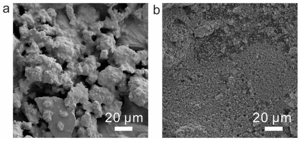
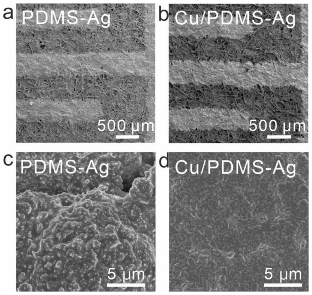
[0046] Ag nanoparticles capped with rosin are mixed and stirred with 3-aminopropyltriethoxysilane solution accounting for 5% of the mass of Ag to form a silane molecular film by self-assembly on the surface of the Ag particles. The polydimethylsiloxane prepolymer (Dow Corning, sylgard 184) and the curing agent (small molecule silane) were mixed in a mass ratio of 10:1, and the above-treated silver nanoparticles (particle size 50% of the total mass) were added. 60-100 nanometers), the mixture of the three is fully stirred until the mixture is uniform to obtain ink. The ink with a certain pattern is printed on the surface of the qualitative filter paper by the screen printing process (the width of the hollow line is 500 microns and the line spacing is 500 microns), and the thickness is about 8 microns, and it is dried at 80 ° C for 2 hours; Immerse i...

Embodiment 2

[0051] Ag nanoparticles capped with rosin are mixed and stirred with 3-aminopropyltriethoxysilane solution accounting for 5% of the mass of Ag to form a silane molecular film by self-assembly on the surface of the Ag particles. Mix the polydimethylsiloxane prepolymer and the curing agent (small molecular silane) in a mass ratio of 10:1, and add the above-treated silver nanoparticles (with a particle size of 60 to 100 nanometers) that account for 50% of the total mass. ), the mixture of the three is fully stirred until the mixture is uniform to obtain ink. A large-area ink pattern with a length of 10 cm and a width of 10 cm was printed on the surface of the qualitative filter paper by a large-area screen printing process, with a thickness of about 8 microns, and dried at 80 °C for 2 hours; the filter paper printed with PDMS-Ag ink was immersed in Swell in tetrahydrofuran solution for 15 minutes; then immerse the swollen substrate in electroless copper plating solution for 30 mi...

Embodiment 3

[0058] This embodiment provides a method for preparing a flexible conductive metal pattern, which includes the following steps:

[0059] Mix the polydimethylsiloxane prepolymer with the curing agent (small molecular silane) in a mass ratio of 10:1, add 60% of the total mass of nickel nanoparticles (the particle size is less than 100 nanometers), and mix the three The mixture was sonicated for 30 minutes and stirred well to obtain ink. The ink with a certain pattern is printed on the surface of the dust-free paper by the screen printing process (the width of the hollow line is 500 microns and the line spacing is 500 microns), and the thickness is about 9 microns. The filter paper was immersed in the acetone solution to swell for 10 minutes; then the swollen substrate was immersed in the electroless nickel plating solution for 1 hour, and the A component of the electroless nickel plating solution was: Ni 2 SO 4 ·5H 2 O (40 g / L), sodium citrate (20 g / L), lactic acid (10 g / L); ...


PUM

PropertyMeasurementUnit
diameteraaaaaaaaaa
particle diameteraaaaaaaaaa
electrical resistanceaaaaaaaaaa

Abstract

The invention is applicable to the technical field of electronic device preparation, and provides a flexible conductive metal pattern and a preparation method, application and conductive material thereof. The preparation method of the conductive metal pattern comprises the following steps: The metal nano-powder, the polydimethylsiloxane prepolymer and the curing agent are mixed with or without the first solvent to obtain ink; the ink is printed on the flexible substrate and cured to obtain the printed substrate; After the substrate is immersed in a second solvent that is miscible with water and can swell ink for swelling treatment, it is then transferred to a metal salt solution to achieve pattern metallization by electroless plating, and then dried to obtain the conductive metal. pattern. The preparation method provided by the invention has simple process and low cost, adopts printing and solution processing methods compatible with industrial preparation methods, and the prepared flexible conductive metal pattern has strong bonding force with the substrate, high conductivity and high printing precision.

Description

technical field [0001] The invention belongs to the technical field of electronic device preparation, and in particular relates to a flexible conductive metal pattern and a preparation method and application thereof. Background technique [0002] At present, various emerging electronic devices have tended to be flexible, including flexible circuit boards, radio frequency identification cards, sensors, displays, solar cells, energy storage devices, smart textiles, electronic skins, and so on. Conductive materials are essential in flexible electronics, so the development of bendable or foldable high-performance flexible conductors is of great significance for various new application scenarios. Flexible conductive materials include metal thin films, carbon-based materials, oxides, two-dimensional transition metal carbides, nitrides and carbonitrides, conductive polymers (polyaniline, polypyrrole, polythiophene), and the like. Compared with other materials, metals have the char...

Claims


Application Information

Patent Timeline
Patent Type & Authority Patents(China)
IPC IPC(8): H01B13/00H01B5/14
CPCH01B13/0026H01B5/14Y02E10/549
Inventor 郭瑞生李昊东王浩然
Owner NORTHWESTERN POLYTECHNICAL UNIV
Why Eureka
Try Eureka