Supercharge Your Innovation With Domain-Expert AI Agents!

Silicon carbide crystal and preparation method thereof

A technology of silicon carbide and crystal, which is applied in the field of silicon carbide crystal and its preparation, can solve the problems of crystal growth rate limitation, incapability of large-scale use, increasing crystal graphitization, etc., to reduce crystal defects, increase sublimation rate and Utilization rate, effect of reducing interference

Active Publication Date: 2021-07-23
SICC CO LTD
View PDF5 Cites 1 Cited by
  • Summary
  • Abstract
  • Description
  • Claims
  • Application Information

AI Technical Summary

Problems solved by technology

Graphitization of silicon carbide raw materials is a common instability factor, which will increase the possibility of crystal graphitization and the formation of other defects, so that the crystal growth rate is largely limited
[0004] The current solution is to add additional solid silicon to the graphite crucible, which can compensate for the lack of silicon in the growth material and prevent the graphitization of the growth material to a certain extent, but this will lead to the formation of liquid silicon droplets and the formation of polymorphic structures. The second is to use tantalum crucibles to create an environment for adsorbing carbon, which can significantly inhibit the graphitization of growth raw materials, but the price of tantalum crucibles is too high to be used on a large scale

Method used


Image

  • Silicon carbide crystal and preparation method thereof
  • Silicon carbide crystal and preparation method thereof
  • Silicon carbide crystal and preparation method thereof

Examples


Embodiment 1

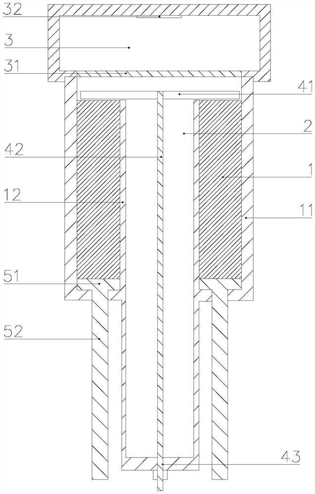
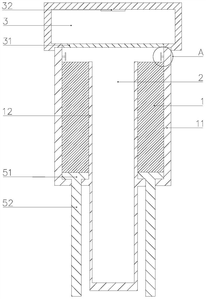
[0093] refer to Figure 1-3 , the embodiment of the application discloses a kind of reactor assembly that is used for growing crystal, and this reactor assembly comprises reaction chamber, crystal growth chamber 3 and material removing mechanism; Reaction chamber comprises raw material chamber 1 and waste material chamber 2, and crystal growth chamber 3 communicates with the raw material chamber 1 through the gas phase transmission channel, and the raw material gas generated by the sublimation of the raw material in the raw material chamber 1 is transported to the crystal growth chamber 3 through the gas phase transmission channel, and the material removal mechanism removes the gas generated during the crystal growth process in the raw material chamber 1 The waste is transferred to waste chamber 2.

[0094] Specifically, the raw material cavity 1 and the waste material cavity 2 are separate chambers, and the separate raw material cavity 1 and the waste material cavity 2 can be...

Embodiment 2

[0124] refer to Figure 4 The difference between this embodiment and Embodiment 1 is that the waste chamber 2 is sleeved on the periphery of the raw material chamber 1, and the waste chamber 2 is formed between the reaction chamber outer cylinder 11 and the reaction chamber inner cylinder 12, and the reaction chamber inner cylinder 12 forms the raw material chamber 1. In this setting mode, the top of the raw material chamber 1 is a high-temperature area, and the raw material is sublimated to grow crystals. The material removal mechanism removes the waste in the raw material chamber 1 in time, so that the waste falls into the bottom of the waste chamber 2. At this time, the waste is far away from the high-temperature area and cannot Continue to be sublimated by heat, avoid crystal defects caused by waste materials, and further improve the growth quality of crystals.

[0125] As an embodiment, the material receiving platform 51 pushes the raw material in the raw material chambe...

Embodiment 3

[0128] In an embodiment not shown, the raw material chamber 1 is formed between the reaction chamber outer cylinder 11 and the reaction chamber inner cylinder 12, and the waste material chamber 2 is arranged at the bottom, the top of the raw material chamber 1 or the outside of the reaction chamber outer cylinder 11, inside the reaction chamber The porosity of the surface of the cylinder 12 is higher than that of the surface of the reaction chamber outer cylinder 11. The seed crystal is arranged in the reaction chamber inner cylinder 12 in the form of a column. The extension direction of the seed crystal and the central axis of the reaction chamber inner cylinder 12 is roughly the same. A crystal growth chamber 3 is formed between the crystal and the inner side wall of the reaction chamber inner cylinder 12, and the heating device is arranged on the outside of the reaction chamber outer cylinder 11, so that the raw material gas in the raw material chamber 1 passes through the re...


PUM

PropertyMeasurementUnit
Widthaaaaaaaaaa
Heightaaaaaaaaaa
Widthaaaaaaaaaa

Abstract

The invention discloses a preparation method of a silicon carbide crystal, and belongs to the field of semiconductor material preparation. The method comprises the steps: providing a reaction cavity, a crystal growth cavity and a material removing mechanism, wherein the reaction cavity comprises a raw material cavity and a waste material cavity, and a silicon carbide raw material is put into the raw material cavity; executing the crystal growth stage: controlling crystal growth conditions, conveying raw material gas generated by sublimation of the raw materials in the raw material cavity to the crystal growth cavity through a gas phase conveying channel for crystal growth, when the sublimation rate of the silicon carbide raw materials is a first sublimation rate, starting a material removing mechanism so that the material removing mechanism transfers waste generated after sublimation of the raw materials in the reaction cavity to a waste cavity, enabling remaining raw materials in the raw material cavity to continue to sublimate under the crystal growth condition for crystal growth, enabling the material removing mechanism to continue to remove materials till crystal growth is finished, and preparing the silicon carbide crystals. The sublimation rate and the utilization rate of the raw materials can be improved, and the defects of crystals are reduced.

Description

technical field [0001] The application relates to a silicon carbide crystal and a preparation method thereof, belonging to the field of semiconductor material preparation. Background technique [0002] At present, in the preparation of silicon carbide crystals, physical vapor transport (PVT method for short) technology is mainly used, which decomposes silicon carbide raw materials into gas phase components Si by sublimation. m C n Finally, driven by the axial temperature gradient, it is transported to the seed crystal and grows into silicon carbide crystals. The PVT method is a complex process, and many parameters must be comprehensively controlled, such as growth temperature, temperature gradient, direct distance between the seed crystal and the growth material, gas pressure, etc. If any parameter is not well controlled, the stability of crystal growth Sex will be destroyed. [0003] In the later stage of the growth of silicon carbide crystals, the silicon carbide raw ma...

Claims


Application Information

Patent Timeline
IPC IPC(8): C30B29/36C30B23/00
CPCC30B29/36C30B23/00
Inventor 刘鹏飞刘星刘家朋李加林
Owner SICC CO LTD
Features
  • R&D
  • Intellectual Property
  • Life Sciences
  • Materials
  • Tech Scout
  • Unparalleled Data Quality
  • Higher Quality Content
  • 60% Fewer Hallucinations
Learn More