Processing technology of IBC battery with passivation contact structure

A technology of processing technology and contact structure, which is applied in the field of IBC battery processing technology, can solve the problems of metal-induced recombination increase in the grid line area, reduce battery passivation effect, and reduce battery efficiency, so as to reduce metal-induced recombination and improve battery efficiency. Efficiency, effect of reducing printing steps

Pending Publication Date: 2021-08-20
ZHEJIANG AIKO SOLAR ENERGY TECH CO LTD +2
View PDF9 Cites 2 Cited by
  • Summary
  • Abstract
  • Description
  • Claims
  • Application Information

AI Technical Summary

Problems solved by technology

[0005] The invention provides a processing technology for an IBC battery with a passivation contact structure, aiming at solving the problem of using a high-temperature sintering slurry to etch the passivation layer to realize the ohmic contact between the gate line and the polysilicon in the IBC battery with a passivation contact structure in the prior art. There is a problem that the high-temperature paste is easy to damage the tunnel oxide layer and reduce the passivation effect of the battery, and the high-temperature paste is easy to damage the polysilicon, which leads to the increase of metal-induced recombination in the gate line area and reduces the battery efficiency.

Method used


Image

  • Processing technology of IBC battery with passivation contact structure
  • Processing technology of IBC battery with passivation contact structure
  • Processing technology of IBC battery with passivation contact structure

Examples


Embodiment 1

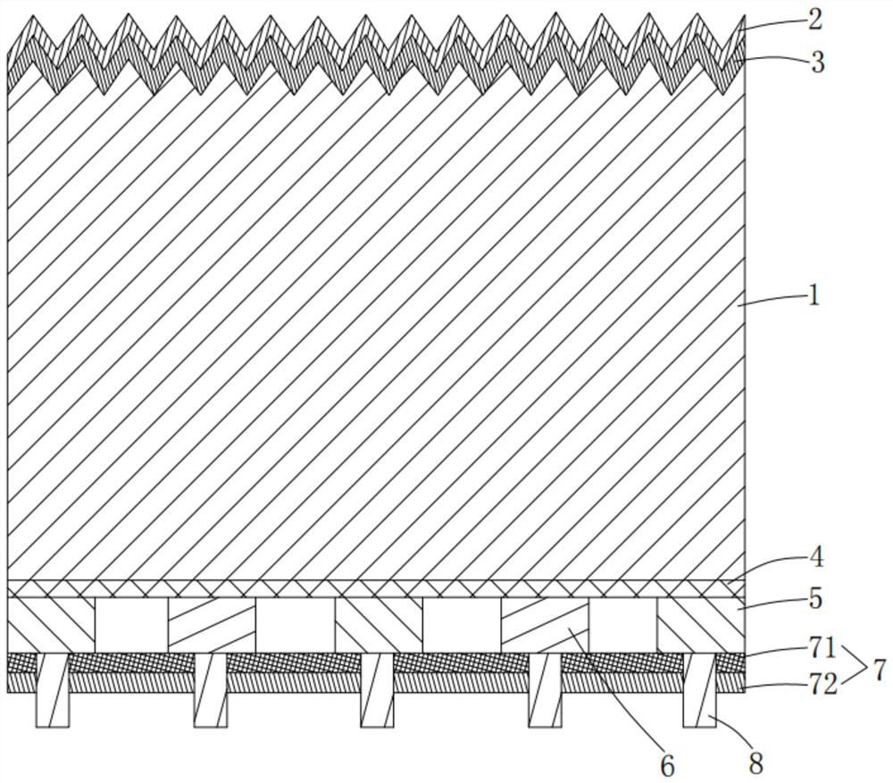
[0028] Please refer to figure 1 , the present embodiment provides an IBC battery with a passivated contact structure, comprising: an N-type monocrystalline silicon wafer 1, and the front of the N-type monocrystalline silicon wafer 1 is sequentially provided with an anti-reflection layer 2 and an N+ doped layer from top to bottom. 3. On the back of the N-type monocrystalline silicon substrate 1, tunnel oxide layers 4, N-type doped polysilicon 5 and P-type doped polysilicon 6, passivation layer 7, and N-type doped polysilicon 6 are arranged in sequence from top to bottom. The backs of the polysilicon 5 and the P-type doped polysilicon 6 are respectively provided with gate lines 8, wherein the gate lines 8 on the back side of the P-type doped polysilicon 6 are positive gate lines, and the positive gate lines form an ohmic contact with the P-type doped polysilicon 6; The gate line 8 on the back of the N-type doped polysilicon 5 is a negative gate line, which forms an ohmic contact...

Embodiment 2

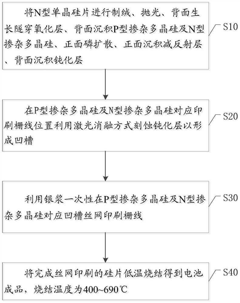
[0031] Please refer to figure 2 , the present embodiment provides a processing technology for an IBC battery with a passivated contact structure, which is used to prepare the IBC battery with a passivated contact structure in the first embodiment, comprising the following steps:

[0032] Step S10, texturing and polishing the N-type single crystal silicon wafer 1, growing a tunnel oxide layer 4 on the back side, depositing P-type doped polysilicon 6 and N-type doped polysilicon 5 on the back side, diffusing phosphorus on the front side, and depositing an anti-reflection layer on the front side 2. Deposit a passivation layer 7 on the back;

[0033] In this step, the N-type monocrystalline silicon wafer 1 is selected as the silicon wafer substrate, and the N-type monocrystalline silicon wafer 1 is textured by wet etching technology, so as to form a textured surface on the back and front of the N-type monocrystalline silicon wafer 1 , to reduce the reflection of light, which is ...

Embodiment 3

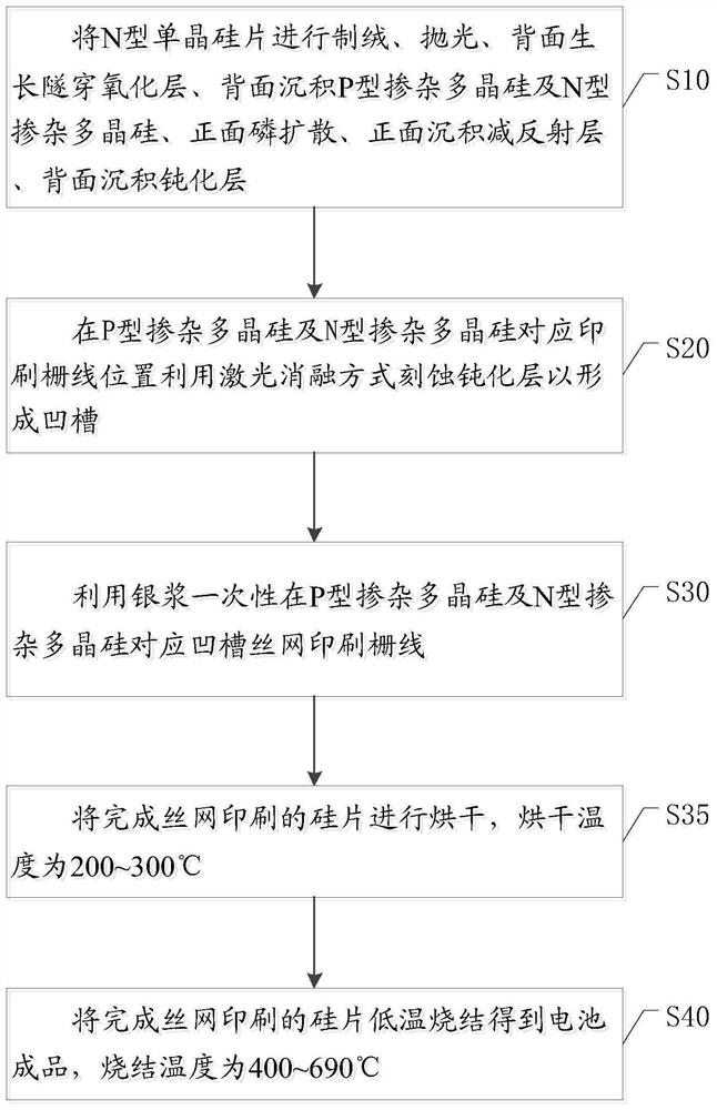
[0051] Please refer to image 3 , on the basis of Example 2, before the step of completing the low-temperature sintering of the screen-printed silicon wafer to obtain the finished battery, it also includes:

[0052] Step S35, drying the screen-printed silicon wafer at a temperature of 200-300°C.

[0053] In this embodiment, before the low-temperature sintering, the screen-printed silicon wafer is dried at a temperature of 200-300° C., which facilitates the subsequent low-temperature sintering process.

[0054] The embodiment of the present invention provides a processing technology of an IBC battery with a passivated contact structure by using laser ablation to etch the passivation layer at the positions corresponding to the printed grid lines of P-type doped polysilicon and N-type doped polysilicon to form grooves, Then use the silver paste to screen-print grid lines in the corresponding grooves of P-type doped polysilicon and N-type doped polysilicon at one time, and sinter...


PUM

PropertyMeasurementUnit
thicknessaaaaaaaaaa
thicknessaaaaaaaaaa

Abstract

The invention is applicable to the technical field of solar cells, and provides a processing technology of an IBC battery with a passivation contact structure. The technology comprises the following steps: texturing and polishing an N-type monocrystalline silicon wafer, growing a tunneling oxide layer on the back surface, depositing P-type/N-type doped polycrystalline silicon on the back surface, performing phosphorus diffusion on the front surface, depositing an antireflection layer on the front surface, and depositing a passivation layer on the back surface; etching the passivation layer at the position of the P-type/N-type doped polycrystalline silicon printing grid line by using laser ablation to form a groove; utilizing silver paste to carry out silk-screen printing on grid lines in the groove corresponding to the P-type/N-type doped polycrystalline silicon at one time; and sintering at a low temperature of 400-690 DEG C to obtain a battery finished product. According to the processing technology of the IBC battery with the passivation contact structure, the groove is etched at the position of the P-type/N-type doped polycrystalline silicon printing grid line through laser ablation, ohmic contact between the grid line and the polycrystalline silicon can be achieved through low-temperature sintering, damage to the polycrystalline silicon and the tunneling oxide layer is avoided, the passivation effect of the battery is ensured, and metal induced recombination in a grid line area is reduced, and the battery efficiency is improved.

Description

technical field [0001] The invention relates to the technical field of solar cell processing, in particular to a processing technology of an IBC cell with a passivation contact structure. Background technique [0002] With the development of solar cell technology, more and more attention has been paid to the reliability of solar cells. Among them, the IBC (Interdigitated back contact) battery is a solar cell in which both P-type doped polysilicon and N-type doped polysilicon are placed on the back of the battery. In order to reduce the surface recombination rate of the battery, the general IBC battery usually uses silicon nitride , silicon dioxide and other films for surface passivation, the use of passivation structure can reduce the surface recombination rate, which is helpful to increase the open circuit voltage. [0003] In the prior art, the processing technology of an IBC battery with a passivated contact structure is usually: N-type monocrystalline silicon wafers are...

Claims


Application Information

Patent Timeline
Patent Type & Authority Applications(China)
IPC IPC(8): H01L31/18H01L31/0224H01L31/0216H01L31/068
CPCH01L31/1804H01L31/1868H01L31/022441H01L31/022458H01L31/02167H01L31/02168H01L31/0682Y02P70/50Y02E10/547Y02E10/546
Inventor 郭方箐陈刚
Owner ZHEJIANG AIKO SOLAR ENERGY TECH CO LTD
Why Eureka
Try Eureka