Surface enhanced Raman scattering substrate and preparation method thereof

A surface-enhanced Raman and substrate technology, used in diffusion elements, sputtering, ion implantation, etc., can solve the problems of complex procedures and long-term processing, and achieve good reproducibility and high measurement limit. , the effect of large size

Active Publication Date: 2021-08-24
江苏度微光学科技有限公司
View PDF7 Cites 3 Cited by
  • Summary
  • Abstract
  • Description
  • Claims
  • Application Information

AI Technical Summary

Problems solved by technology

However, these conventional techniques are fundamentally limited by their complex procedures, long processing times, and high manufacturing costs in order to meet the increasing demands of practical applications.

Method used


Image

  • Surface enhanced Raman scattering substrate and preparation method thereof
  • Surface enhanced Raman scattering substrate and preparation method thereof
  • Surface enhanced Raman scattering substrate and preparation method thereof

Examples


Embodiment 1

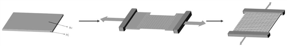
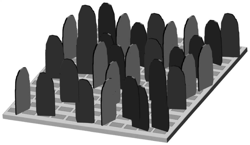
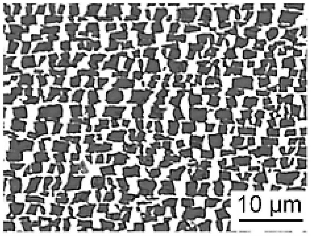
[0036] A layer of gold is deposited on the flexible PEI polymer substrate. The electron beam evaporator is deposited on a golden nanofil film having a thickness of 20 nanometers on a thickness of 125 microns and a length of 10 cm and a width of 10 cm, a width of 10 cm, a smooth surface smooth, so that it becomes a gold / PEI film, deposition rate. for The deposition time was 6 minutes, and the thickness of the gold nano film was 20 nm. During the deposition, the temperature of the vacuum chamber is maintained below 60 ° C to prevent the PEI film from being thermally expanded or deflated due to internal stress, resulting in a gold film to produce defects or wrinkles. After the vapor deposition, dried in an oven at 150 ° C for 30 min, so that the gold nano film and PEI were more combined, and the gold nanofil film was cracked as the crack of the PEI film was determined during subsequent stretching.

[0037] like Figure 1 The X-direction is performed using a gold / PEI film, the str...

Embodiment 2

[0042] A layer of gold is deposited on the flexible PEI polymer substrate. The electron beam evaporator is deposited from a golden nanometers having a thickness of 40 nanometers on a PEI film having a thickness of 125 microns and a length of 10 cm and a width of 10 cm and a width, which becomes a gold / PEI film, deposition rate. for The deposition time was 10 minutes, and the thickness of the gold nano film was 40 nm. During the deposition, the temperature of the vacuum chamber was 55 ° C and dried in an oven at 160 ° C after 20 min after the vapor deposition.

[0043] A piece of gold / PEI film is used for stretching in the X direction, and the stretching speed is 0.02 mm / second, stretched for 15 minutes. The PEI film passes through a necklace process, and stress is applied to the gold film by surface adhesion. When the stress exceeds the mechanical breakage strength, the gold film is broken into a strip. The prepared film was re-stretched in the Y direction to produce a two-...


PUM

PropertyMeasurementUnit
thicknessaaaaaaaaaa
thicknessaaaaaaaaaa

Abstract

The invention discloses a surface enhanced Raman scattering substrate and a preparation method thereof. The method comprises the following steps: firstly, growing a layer of gold nano film on a flexible polymer substrate, and enabling the gold film to generate regular and uniform cracks along with the extension of a polymer through adoption of a two-way mechanical stretching method; and then, transferring the gold film with the stretched microstructure to a clean glass substrate, and a layer of uniform and compact SnSe2 nanosheets grow on the gold film. The structure combines the advantages of a traditional metal SERS substrate, that is, a metal tip has a hot spot, and a local electric field is enhanced; and the two-dimensional material SnSe2 has the advantages that the two-dimensional material SnSe2 and the semiconductor SERS substrate are combined, surface non-uniformity caused by agglomeration due to weak adsorption capacity of the metal SERS substrate can be avoided, in addition, the two-dimensional material SnSe2 is large in specific surface area, the structure has a light limiting effect, and light can be limited in the structure. The advantages of a semiconductor SERS substrate and a traditional metal substrate are combined, and the effect of enhancing Raman scattering is achieved.

Description

Technical field [0001] The present invention relates to the field of Raman spectroscopy, and more particularly to a surface enhanced Raman scattering substrate and a preparation method. Background [0002] Light irradiates, elastic scattering and non-elastic scattering. The elastic scattered scattering light is the same component, and the non-elastic scattered scattered light is compared to the long and short ingredient of the excitation wave, collectively referred to as Raman effect. . [0003] The superiority of Raman spectroscopy can provide fast, simple, repeatable, and more importantly, non-damaged qualitative quantitative analysis, no sample preparation, the sample can be directly measured by fiber optic probe or glass, quartz and optical fiber. Raman spectrum spectrum peak is clear, more suitable for quantitative research, database search, and use differential analysis. Therefore, it is a very useful and reliable scientative analysis method using Raman effects. However, Ra...

Claims


Application Information

Patent Timeline
Patent Type & Authority Applications(China)
IPC IPC(8): G02B5/02C23C14/30C23C14/20C23C16/30C23C28/00
CPCG02B5/0221C23C14/30C23C14/20C23C16/305C23C28/322C23C28/34
Inventor 侯玉欣马庆罗向东余洋陈明
Owner 江苏度微光学科技有限公司
Why Eureka
Try Eureka