Method for improving electrical performance of GaN vertical Schottky diode with strip-shaped groove structure based on self-alignment process

A Schottky diode, self-aligned process technology, applied in diodes, circuits, electrical components, etc., can solve the problems of reducing device performance and application, large reverse leakage, etc.

Pending Publication Date: 2021-09-10
XI AN JIAOTONG UNIV
View PDF9 Cites 0 Cited by
  • Summary
  • Abstract
  • Description
  • Claims
  • Application Information

AI Technical Summary

Problems solved by technology

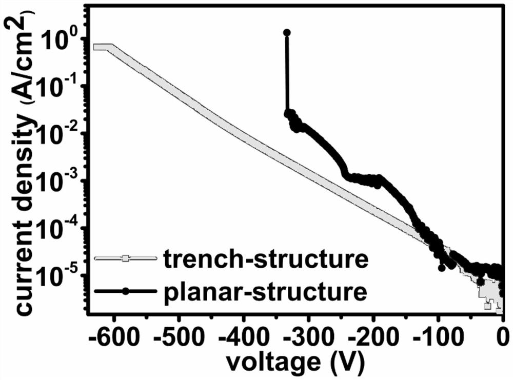
However, an important problem at present is that the reverse leakage of the prepared Schottky diodes is generally large, which makes the device undergo early pre-breakdown under very low reverse bias voltage, which seriously reduces the performance and performance of the device. application, so how to effectively reduce the reverse leakage level is extremely important for expanding the application of GaN Schottky diodes

Method used


Image

  • Method for improving electrical performance of GaN vertical Schottky diode with strip-shaped groove structure based on self-alignment process

Examples


Embodiment 1

[0045] S1 Ultrasonic cleaning the self-supporting substrate GaN in acetone, absolute ethanol, and deionized water in sequence;

[0046] S2. Prepare a mask with an etching thickness of 1 μm in AZ6130 photoresist on the surface of the GaN cleaned in step S1 using a standard photolithography process;

[0047] S3, performing an alignment mark etching experiment on the GaN of the etching mask in step S2 using an inductively coupled plasma ICP dry etching process;

[0048] S4. After the alignment mark etching in step S3 is completed, the Ti / Al / Ni / Au metal layer is evaporated on the back of the GaN substrate by electron beam technology, with a thickness of 200nm, and is treated by RTA rapid annealing equipment at 750°C and Ar environment 20s to form a corresponding ohmic contact;

[0049] S5. Use photolithography and electron beam technology to make ohmic contact with the prepared GaN substrate front side in step S4, and prepare a strip-shaped metal Ni mask with a thickness of 200nm...

Embodiment 2

[0055] S1 Ultrasonic cleaning the self-supporting substrate GaN in acetone, absolute ethanol, and deionized water in sequence;

[0056] S2. Prepare a mask with an etching thickness of 1.5 μm of AZ6130 photoresist on the surface of the GaN cleaned in step S1 by a standard photolithography process;

[0057] S3, performing an alignment mark etching experiment on the GaN of the etching mask in step S2 using an inductively coupled plasma ICP dry etching process;

[0058] S4. After the etching of the alignment mark in step S3 is completed, a Ti / Al / Ni / Au metal layer is evaporated on the back of the GaN substrate by an electron beam process, with a thickness of 300nm, and is treated by RTA rapid annealing equipment at 850°C and Ar environment 30s to form a corresponding ohmic contact;

[0059] S5. Using photolithography and electron beam technology to ohm-contact the front side of the prepared GaN substrate in step S4, prepare a 300nm strip-shaped metal Ni mask, and the corresponding...

Embodiment 3

[0065] S1 Ultrasonic cleaning the self-supporting substrate GaN in acetone, absolute ethanol, and deionized water in sequence;

[0066] S2. Prepare a mask with an etching thickness of 1.2 μm of AZ6130 photoresist on the surface of the GaN cleaned in step S1 by using a standard photolithography process;

[0067] S3, performing an alignment mark etching experiment on the GaN of the etching mask in step S2 using an inductively coupled plasma ICP dry etching process;

[0068] S4. After the alignment mark etching in step S3 is completed, the Ti / Al / Ni / Au metal layer is evaporated on the back of the GaN substrate by electron beam technology, with a thickness of 240nm, and is treated by RTA rapid annealing equipment at 790°C and Ar environment 24s to form a corresponding ohmic contact;

[0069] S5. Use photolithography and electron beam technology to make ohmic contact with the front side of the prepared GaN substrate in step S4, and prepare a 240nm strip-shaped metal Ni mask, and th...


PUM

PropertyMeasurementUnit
thicknessaaaaaaaaaa
thicknessaaaaaaaaaa
thicknessaaaaaaaaaa

Abstract

The invention discloses a method for improving the electrical performance of a GaN vertical Schottky diode with a strip-shaped groove structure based on a self-alignment process. The method comprises the following steps: preparing a photoresist etching mask on the front surface of a self-supporting substrate GaN by adopting a standard photoetching process, performing an alignment mark etching experiment on the self-supporting substrate GaN by adopting an inductively coupled plasma (ICP) dry etching process, carrying out vacuum evaporating of a Ti / Al / Ni / Au metal layer on the back surface of the self-supporting GaN substrate by adopting an electron beam process, and carrying out rapid annealing treatment to form ohmic contact, preparing a strip-shaped metal Ni mask on the front surface of the self-supporting GaN substrate by adopting photoetching and electron beam processes, etching the strip-shaped metal Ni mask by adopting an ICP (Inductively Coupled Plasma) dry etching process, and injecting Ar ions into the front surface of the self-supporting substrate GaN, and finally, preparing a Ni / Al composite metal layer on the front surface of the self-supporting GaN substrate after ion implantation to form the GaN Schottky diode with a metal-insulating layer-semiconductor structure. According to the invention, the reverse electric leakage of a common vertical GaN Schottky diode can be effectively reduced, and the breakdown voltage is improved.

Description

technical field [0001] The invention belongs to the technical field of wide bandgap semiconductor devices, and in particular relates to a method for improving the electrical performance of a GaN vertical Schottky diode with a strip-shaped trench structure based on a self-alignment process. Background technique [0002] The third-generation wide-bandgap semiconductor material represented by gallium nitride (GaN) is rapidly becoming the material of choice for high-frequency and high-power devices due to its high critical breakdown field strength and high electron saturation drift velocity. Especially in the field of power diode rectifier devices, it has important application prospects. As an important two-terminal electronic component, Schottky diode (SBD) has important applications in circuits such as detection and frequency mixing. However, an important problem at present is that the reverse leakage of the prepared Schottky diodes is generally large, which makes the device u...

Claims


Application Information

Patent Timeline
Patent Type & Authority Applications(China)
IPC IPC(8): H01L21/28H01L21/329H01L29/47H01L29/872
CPCH01L29/66212H01L29/401H01L29/475H01L29/8725
Inventor 耿莉刘江杨明超刘卫华韩传余郝跃
Owner XI AN JIAOTONG UNIV
Why Eureka
Try Eureka