Preparation method of perovskite solar cell with GaN semiconductor material as dual-function layer

A solar cell and perovskite technology, applied in semiconductor/solid-state device manufacturing, semiconductor devices, organic semiconductor devices, etc., to achieve high photoelectric conversion efficiency, improve photoelectric conversion efficiency, and increase light absorption rate

Pending Publication Date: 2021-09-28
SHANDONG UNIV
View PDF14 Cites 1 Cited by
  • Summary
  • Abstract
  • Description
  • Claims
  • Application Information

AI Technical Summary

Problems solved by technology

Although some studies have demonstrated the potential advantages of GaN in the field of perovskite solar cells, such as improved stability or the use of GaN as an ETL material in current devices, however, in the field of perovskite solar cells, the elimination of unwanted heterogeneous interface, simplify the device manufacturing process, and expand its design versatility in devices, GaN materials are likely to produce the greatest benefits

Method used


Image

  • Preparation method of perovskite solar cell with GaN semiconductor material as dual-function layer
  • Preparation method of perovskite solar cell with GaN semiconductor material as dual-function layer
  • Preparation method of perovskite solar cell with GaN semiconductor material as dual-function layer

Examples


Embodiment 1

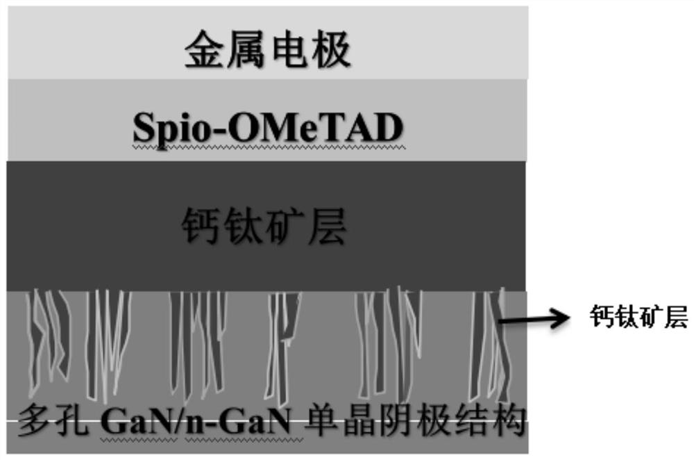
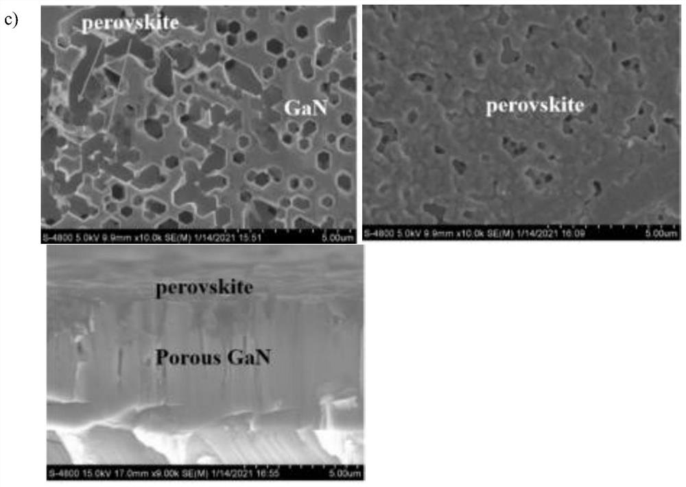
[0038] A perovskite solar cell based on a porous GaN / n-GaN single crystal as a double functional layer, including a single crystal double functional layer cathode structure, a perovskite layer, a hole transport layer and a metal counter electrode layer from bottom to top. structured as figure 1 shown.

[0039] GaN semiconductor material is used as the preparation method of the perovskite solar cell of bifunctional layer, and the steps are as follows:

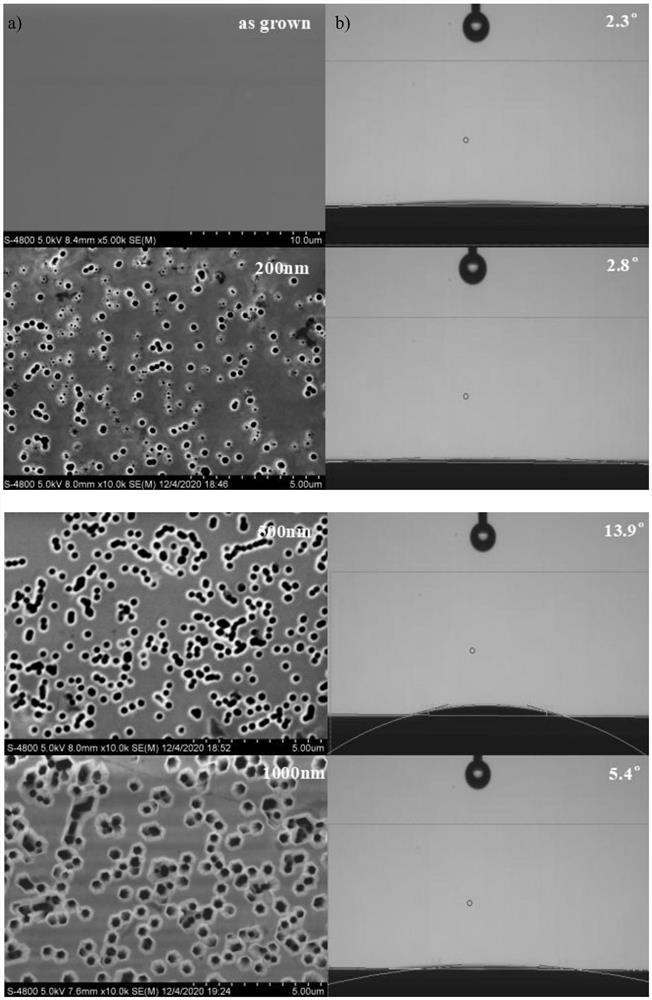
[0040] (1) The substrate of n-type GaN thin film grown on double-sided polished sapphire substrate by MOCVD method is cleaned in sequence with acetone, IPA and deionized water in an ultrasonic bath for 10 minutes; the substrate is placed in a high-temperature atmosphere furnace Perform high temperature annealing, the annealing gas is high-purity N 2 Gas, annealing temperature 1100°C, annealing time 30min, porous GaN / n-GaN single crystal is obtained after annealing; SEM image and contact angle test results of porous GaN / n-GaN s...

Embodiment 2

[0047] A method for preparing a GaN semiconductor material as a perovskite solar cell with a double functional layer, the steps are as follows:

[0048] (1) The substrate of n-type GaN thin film grown on double-sided polished sapphire substrate by MOCVD method is cleaned in sequence with acetone, IPA and deionized water in an ultrasonic bath for 10 minutes; the substrate is placed in a high-temperature atmosphere furnace Perform high temperature annealing, the annealing gas is high-purity N 2 Gas, annealing temperature 1150°C, annealing time 60min, porous GaN / n-GaN single crystal is obtained after annealing;

[0049] (2) Clean the porous GaN / n-GaN single crystal substrate in an ultrasonic bath with acetone, IPA and deionized water for 10 minutes, and then treat it with oxygen plasma for 15 minutes;

[0050] (3) in N 2 In the glove box, 100 mL of the perovskite precursor solution was spin-coated onto the porous GaN / n-GaN single wafer at a speed of 4000 rpm for 45 s, and then ...

Embodiment 3

[0055] A method for preparing a GaN semiconductor as a perovskite solar cell with a double functional layer, the steps are as follows:

[0056] (1) The substrate of n-type GaN thin film grown on double-sided polished sapphire substrate by MOCVD method is cleaned in sequence with acetone, IPA and deionized water in an ultrasonic bath for 10 minutes; the substrate is placed in a high-temperature atmosphere furnace Perform high temperature annealing, the annealing gas is high-purity N 2 Gas, annealing temperature 1120°C, annealing time 90min, porous GaN / n-GaN single crystal is obtained after annealing;

[0057] (2) Clean the porous GaN / n-GaN single crystal substrate in an ultrasonic bath with acetone, IPA and deionized water for 10 minutes, and then treat it with oxygen plasma for 15 minutes;

[0058] (3) in N 2 In the glove box, 100 mL of the perovskite precursor solution was spin-coated onto the porous GaN / n-GaN single wafer at a speed of 4000 rpm for 45 s, and then 200 mL of...


PUM

PropertyMeasurementUnit
thicknessaaaaaaaaaa
thicknessaaaaaaaaaa
thicknessaaaaaaaaaa

Abstract

The invention relates to a preparation method of a perovskite solar cell with a GaN semiconductor material as a dual-function layer, and the method comprises the steps: carrying out high-temperature annealing on a substrate to obtain a porous GaN / n-GaN single-crystal substrate; sequentially subjecting the porous GaN / n-GaN single crystal substrate to oxygen plasma vacuum treatment, perovskite light absorption layer coating, hole transport layer coating and electrode evaporation. According to the method, a porous GaN / n-GaN single crystal is used as a dual-functional-layer cathode structure of the perovskite solar cell, is used as a transparent conductive layer and an electron transport layer, and does not have an independent conductive glass layer; and the porous structure of the porous GaN single crystal provides an extended interface contact area with the perovskite light absorber, and shows high light transmittance in a visible spectrum. As the interface with the perovskite is enlarged, the light collection effect is enhanced, and effective carrier extraction is provided. Meanwhile, the porous GaN single crystal is used as the electron transport layer, so that more active positions can be provided, and the light absorptivity can be improved.

Description

technical field [0001] The invention relates to a method for preparing a perovskite solar cell with a GaN semiconductor material as a double-functional layer, belonging to the technical field of semiconductor devices. Background technique [0002] Due to the excellent performance of perovskite solar cells (PSCs), the halide perovskite AMX 3 (where A=CH 3 NH 3 + , CH(NH 2 ) 2 + , Cs + ;M=Pb 2+ , Sn 2+ ;X=I - , Br - , Cl - ) has become a frontier material for optoelectronic materials. Bandgap tunability (1.5-3.1eV), high absorption coefficient (10 4 -10 5 cm -1 ), low exciton binding energy (<50 meV), and facile fabrication method play key roles in solidifying halide perovskite sites in solar cells. However, since the dopant-host interaction in perovskite is different from conventional semiconductor materials (such as Si:B, GaAs:Mg, AlN:Si), perovskite has not been doped to form p-i-n junction. Therefore, integration of heterogeneous materials is required ...

Claims


Application Information

Patent Timeline
Patent Type & Authority Applications(China)
IPC IPC(8): H01L51/48H01L51/46H01L51/44
CPCH10K71/00H10K71/60H10K30/81H10K30/82H10K2102/00Y02E10/549
Inventor 张雷李秋波俞娇仙刘光霞王国栋陈成敏刘鑫彤王泰林赵刚
Owner SHANDONG UNIV
Why Eureka
Try Eureka