Method for manufacturing conductive pattern by selectively activating insulating material by using laser

An insulating material and selective technology, applied in manufacturing tools, laser welding equipment, printed circuit manufacturing, etc., can solve the problems of high cost of substrates, heavy environmental burden, and changes, and achieve high pass rate and less overflow plating. Effect

Pending Publication Date: 2021-10-29
德中(天津)技术发展股份有限公司
View PDF13 Cites 0 Cited by
  • Summary
  • Abstract
  • Description
  • Claims
  • Application Information

AI Technical Summary

Problems solved by technology

[0017] Generally speaking, there are roughly three types of 3D-MID process technologies that use laser processing: (1) Doping active materials in plastics, laser selective processing, releasing only active groups in the conductive pattern area, and regional chemical plating , the base material cost of this kind of technology is high, compared with the base material without active material, the chemical, physical, electrical and other properties will change; (2) global activation, chemical plating, use laser to remove conductive material, and carry out surface treatment on the workpiece surface Electrical partitioning, local electroplating, such technologies require chemical roughening of the surface of insulating materials, which are half-reduction methods and have a large environmental burden; (3) lasers are used directly or indirectly to make roughened surfaces in conductive pattern areas, And laser selective coating of conductive materials. Although this method is aware of the effect of roughening on adhesion, there are still technical details to be solved, especially when it comes to the selection of laser parameters. More, quantifiable, actionable information

Method used


Image

  • Method for manufacturing conductive pattern by selectively activating insulating material by using laser
  • Method for manufacturing conductive pattern by selectively activating insulating material by using laser
  • Method for manufacturing conductive pattern by selectively activating insulating material by using laser

Examples


Embodiment 1

[0075] The material of this example is an ordinary grade ABS plastic board, and the ABS material is a polymer of three monomers of acrylonitrile (Acrylonitrile), 1,3-butadiene (Butadiene), and styrene (Styrene).

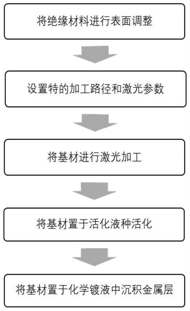
[0076] (1) Surface adjustment of the ABS base material.

[0077] The surface adjustment treatment process is preferably plasma treatment, the gas ratio is preferably: nitrogen / oxygen / carbon tetrafluoride = 1 / 8 / 2, the temperature is 30-70 degrees Celsius, and the treatment time is 1-3 minutes. The hydrophilicity of the treated ABS substrate increases, but the adsorption of colloidal palladium is weakened.

[0078] (2) Set the processing path and laser parameters.

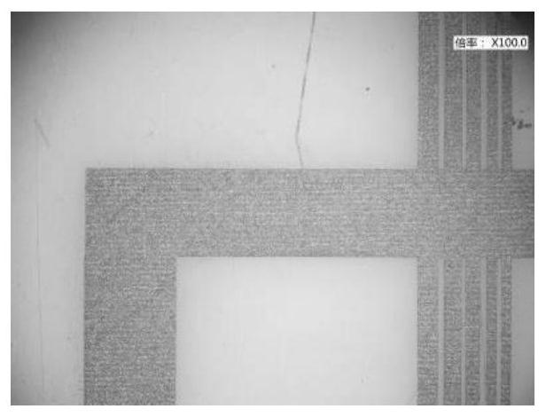
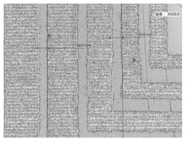
[0079] In this embodiment, the DirectLaser 600P ultraviolet picosecond laser machine produced by Dezhong (Tianjin) Technology Development Co., Ltd. is preferably used to carry out the laser processing test. The power is preferably 40-90%. The corresponding pit diameters after single pulse or pulse train p...

Embodiment 2

[0097] The material of this example uses PC (40%)+ABS plastic alloy.

[0098] (1) Coat the PC (40%)+ABS material surface with a coating.

[0099] The type of coating is preferably silicone resin, and the solid content of the prepared solution is 2%-6%. Coating by dipping, time 3-10s, room temperature.

[0100] Use Dyne to test surface tension. The surface tension of the material was 36 before coating and dropped to 32 after coating. Observation and comparison under a microscope shows that there are micropits invisible to the naked eye on the surface of the substrate before coating, and the micropits are filled after coating.

[0101] (2) Set the processing path and laser parameters.

[0102] In this embodiment, the DirectLaser U5 ultraviolet nanosecond laser machine produced by Dezhong (Tianjin) Technology Development Co., Ltd. is preferably used for laser processing. This device has a zoom beam expander system.

[0103] The initial beam expansion factor is 3 times, and ...


PUM


Abstract

The invention relates to a method for manufacturing a conductive pattern by selectively activating an insulating material by using laser. The method comprises the following steps of that the surface of the insulating material is adjusted to enable the surface to be in a state which is not favorable for depositing an activating agent; and a specific processing path and laser parameters are set, tiny pits in a certain arrangement are formed in the surface subjected to laser processing, any two pits cannot be overlapped, the surface of a base material is selectively processed by the laser according to an electronic pattern, and the adjusted surface state is selectively damaged. The base material is placed in an activating solution, the surface adjustment and pit effects are accumulated, and therefore the activating agent is selectively deposited on a laser-machined part; and the base material is placed in a chemical plating solution to deposit a metal layer, and a metal circuit of an electronic pattern is formed on the surface of the base material after the deposition is finished. Due to the fact that the surface is adjusted in advance, the overflow plating problem is better controlled, and the method can be applied to a finer circuit. A microscopic pit structure after laser processing can ensure that enough binding force exists between the metal layer and the base material even if chemical coarsening is not needed.

Description

technical field [0001] The invention belongs to the field of insulating materials, and relates to conductor structure manufacturing (3D-MID) technology, in particular to a method and components for selectively forming electronic patterns on insulating materials. Background technique [0002] With the improvement of the integration of electronic equipment, the volume of the equipment is getting smaller and smaller. At this time, the electronic components are too large for the entire equipment, which requires reducing their own size. It is a difficult problem in the development of electronic equipment to reduce the size without significantly affecting the function and efficiency of electronic components, and 3D-MID technology is a type of technology that can better solve this problem. [0003] 3D-MID is the abbreviation of "Three-dimensional Molded Interconnect Device" in English, and the Chinese literal translation is three-dimensional molded interconnect device or electronic...

Claims


Application Information

Patent Timeline
Patent Type & Authority Applications(China)
IPC IPC(8): B23K26/352C23C18/22C23C18/30C23C18/40H05K3/18
CPCB23K26/3584C23C18/1608C23C18/22C23C18/285C23C18/30C23C18/405H05K3/185B23K2103/42
Inventor 王恒亮胡宏宇
Owner 德中(天津)技术发展股份有限公司
Why Eureka
Try Eureka