Ultraviolet band adjustable photoelectric detector with transparent conductive structure and production method of ultraviolet band adjustable photoelectric detector

An ultraviolet band, transparent and conductive technology, applied in the field of photoelectric detection, can solve the problems of poor conductivity of graphene films, failure of photodetectors, increase of dark current, etc., so as to improve conductivity uniformity and alleviate lattice constant mismatch. , the effect of reducing dark current

Inactive Publication Date: 2021-11-12
迪优未来科技(清远)有限公司 +1
View PDF0 Cites 0 Cited by
  • Summary
  • Abstract
  • Description
  • Claims
  • Application Information

AI Technical Summary

Problems solved by technology

[0006] The purpose of the present invention is to provide a new UV band tunable photodetection structure with a transparent conductive structure, which overcomes defects at the contact surface caused by GaN / AlGaN materials due to lattice constant mismatch, and increases the dark current near the interface , resulting in the failure of photodetectors and the deterioration of the conductivity of the graphene film during the transfer process

Method used


Image

  • Ultraviolet band adjustable photoelectric detector with transparent conductive structure and production method of ultraviolet band adjustable photoelectric detector
  • Ultraviolet band adjustable photoelectric detector with transparent conductive structure and production method of ultraviolet band adjustable photoelectric detector
  • Ultraviolet band adjustable photoelectric detector with transparent conductive structure and production method of ultraviolet band adjustable photoelectric detector

Examples


Embodiment 1

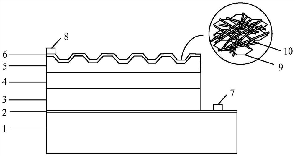
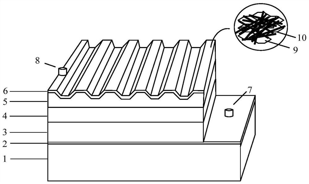
[0036] Refer to attached figure 1 , 2 , the invention discloses an ultraviolet band tunable photodetector with a transparent conductive structure, the structure of the detector is a detector substrate 1, a graphene insertion layer 2, a first GaN layer 3, an AlGaN layer arranged in sequence 4. Ga 2 o 3 Layer 5, transparent conductive layer 6, electrodes are arranged on the graphene insertion layer 2 and transparent conductive layer 6.

[0037] In this embodiment, the transparent conductive layer 6 is a graphene-silver nanowire structure. Refer to attached figure 1 Partially enlarged part of , wherein, the graphene-silver nanowire structure includes: a graphene film 9 and a silver nanowire structure 10 . The hybridization of graphene and silver nanowires can effectively reduce the defects generated during the preparation and transfer of graphene, improve the conductivity uniformity of graphene, and improve the photocurrent and responsivity of the prepared photodetector.

...

Embodiment 2

[0050] On the basis of Example 1, the present invention also discloses a preparation method of an ultraviolet band tunable photodetection structure with a transparent conductive structure, which is characterized in that it includes the following steps:

[0051] In step 1, a single-layer graphene intercalation layer 2 is prepared on metal Cu by a vapor phase deposition method, and the metal Cu is removed to transfer the graphene to a sapphire substrate.

[0052] Step 2, growing a first GaN layer 3 and an AlGaN layer 4 on the graphene insertion layer 2 .

[0053] Step 3, forming an undoped second GaN layer on the AlGaN layer 4, and removing the intrinsic oxide layer of the second GaN layer.

[0054] Step 4, put the second GaN layer from which the intrinsic oxide layer has been removed into a quartz tube furnace, and inject oxygen at high temperature; define a pattern through the photoresist and process it into a ladder shape to obtain a ladder-like GaN layer 2 o 3 Layer 5.

...

Embodiment 3

[0075] On the basis of Embodiment 1, the present invention also discloses an ultraviolet band tunable photodetector with a transparent conductive structure, using the photodetection structure of Embodiment 1.

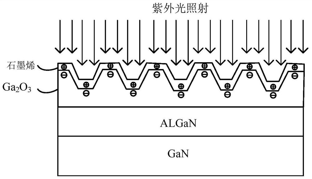
[0076] In this example, refer to the attached Figure 5 And attached Figure 6 , the detection band of the photodetector changes with the applied bias voltage, and the photodetector detects ultraviolet light bands of different wavelengths.

[0077] Since this embodiment is written on the basis of Embodiment 1, the working principle of the photodetection structure will not be described in detail.

[0078] To sum up, the embodiment of the present invention provides a photoelectric detection structure, a photodetector and a preparation method, and the beneficial effects are as follows:

[0079] 1. There is a lattice constant mismatch between the sapphire substrate and the first GaN layer 3, which affects the quality of crystal growth. However, using graphene as the interc...


PUM

PropertyMeasurementUnit
thicknessaaaaaaaaaa
thicknessaaaaaaaaaa

Abstract

The invention belongs to the technical field of photoelectric detection, and discloses an ultraviolet band adjustable photoelectric detector with a transparent conductive structure and a production method of the ultraviolet band adjustable photoelectric detector. The structure of the detector comprises a detector substrate, a graphene insertion layer, a first GaN layer, an AlGaN layer, a Ga2O3 layer and a transparent conductive layer which are sequentially arranged, and electrodes are arranged on the graphene insertion layer and the transparent conductive layer. The detector has the advantages that the graphene serves as the insertion layer and is bonded with the GaN layer through a Van der Waals force, lattice constant mismatch with the sapphire substrate is greatly relieved, dislocation density is reduced, and the growth quality of the epitaxial layer is improved; and compared with a photoelectric detector prepared by a conventional GaN / AlGaN epitaxial structure, the photoelectric detector has the advantages that the ladder-shaped Ga2O3 layer is added, on one hand, the Ga2O3 layer and the transparent conductive layer form a Schottky barrier to reduce a dark current, on the other hand, the ladder-shaped Ga2O3 layer can effectively increase the light receiving area, and the light current is increased in cooperation with the high mobility characteristic of the graphene transparent conductive material.

Description

technical field [0001] The invention relates to the technical field of photoelectric detection, in particular to an ultraviolet band tunable photodetector with a transparent conductive structure and a preparation method thereof. Background technique [0002] At present, ultraviolet light can be divided into far ultraviolet UV-A (315-400nm), medium ultraviolet UV-B (280-315nm), and short ultraviolet UV-C (100-280nm) according to the wavelength. Different wave bands are used in military technology and civilian markets. Fields such as communications and imaging have different values. For example, in the sun-blind area in the atmosphere, the conduction zone tail flame can be used to detect the radiation in the sun-blind ultraviolet band; in the mid-ultraviolet region, space-based ultraviolet early warning can be carried out; in the far ultraviolet region, ultraviolet detection of air targets near the ground can be carried out. probing. The ultraviolet detection can determine t...

Claims


Application Information

Patent Timeline
Patent Type & Authority Applications(China)
IPC IPC(8): H01L31/0304H01L31/0224H01L31/102H01L31/18
CPCH01L31/03048H01L31/03044H01L31/022408H01L31/022466H01L31/102H01L31/1848H01L31/1856Y02P70/50
Inventor 毛明华谢雅芳尹以安
Owner 迪优未来科技(清远)有限公司
Why Eureka
Try Eureka