

Silicon-based AlN capacitor with high withstand voltage and low electric leakage and preparation method thereof
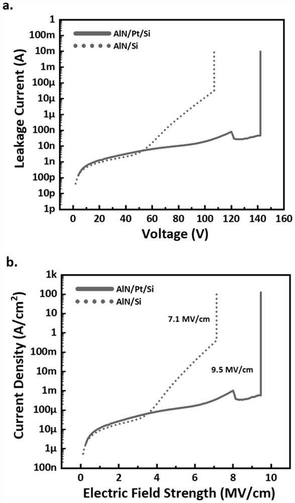
A capacitor and silicon-based technology, which is applied in the field of silicon-based AlN capacitors with high withstand voltage and low leakage and its preparation, can solve the problems of missing N elements in the AlN dielectric layer, and achieve the effects of reducing leakage current, good quality and increasing insulation performance.
- Summary
- Abstract
- Description
- Claims
- Application Information
AI Technical Summary
Problems solved by technology
Method used
Image

Examples
preparation example Construction
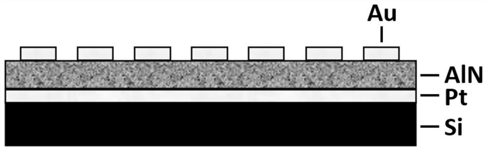
[0050] The preparation method of the silicon-based AlN capacitor comprises the following steps:
[0051] (1) The silicon substrate is cleaned. The silicon substrate is preferably cleaned by RCA standard cleaning process.
[0052] (2) Depositing a Pt buffer layer on the silicon substrate. Specifically, the magnetron sputtering method is used to deposit the Pt buffer layer, and the deposition thickness may be between 5-10 nm.
[0053] (3) Depositing an AlN dielectric thin film on a silicon substrate deposited with a Pt buffer layer. The AlN dielectric thin film is preferably deposited by pulsed laser deposition, and high-purity nitrogen is used as the growth atmosphere.
[0054] (4) Annealing the AlN dielectric thin film. More preferably, in-situ annealing is performed for 30 minutes after the deposition of the AlN dielectric film, and the annealing conditions are to maintain the temperature and nitrogen partial pressure during the deposition of the AlN dielectric film.
[...
Embodiment 1
[0059] Specifically, the silicon-based AlN capacitor is prepared according to the following steps:
[0060] (1) Selection and processing of the silicon substrate: select a low-resistance p-type silicon substrate as the silicon substrate, and use the RCA standard cleaning process to clean the silicon substrate.
[0061] (2) Depositing a Pt buffer layer on a silicon substrate: a Pt buffer layer with a thickness of 5-10 nm is deposited on a silicon substrate by radio frequency magnetron sputtering, the magnetron sputtering power is set to 20-30W, and argon Gas is used as a protective gas, and the atmospheric pressure is 0.1-0.5Pa.
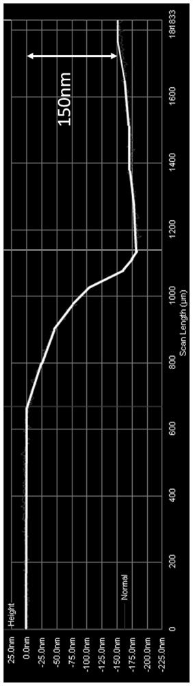
[0062] (3) Depositing an AlN dielectric film on a silicon substrate with a Pt buffer layer deposited: a pulsed laser deposition method is used to deposit an AlN dielectric film with a thickness of 150 nm on a silicon substrate with a Pt buffer layer, and the pulsed laser energy flux density is 2- 2.5J / cm 2 , the laser repetition frequency is 5Hz, th...
PUM
| Property | Measurement | Unit |
|---|---|---|
| thickness | aaaaa | aaaaa |
| thickness | aaaaa | aaaaa |
| breakdown field strength | aaaaa | aaaaa |
Abstract
Description
Claims
Application Information