

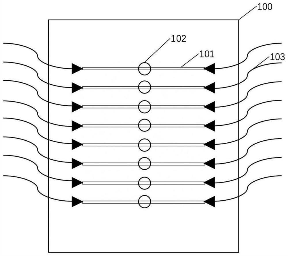
Multi-channel micro-ring sensor and preparation and use method thereof
A sensor and multi-channel technology, applied to instruments, scientific instruments, and material analysis through optical means, can solve the problems of difficult integration of microfluidic chips, application limitations of micro-ring devices, and long time required to achieve simplification Effects of chip preparation and modification process, high integration, and chip size reduction
- Summary
- Abstract
- Description
- Claims
- Application Information
AI Technical Summary
Problems solved by technology
Method used
Image

Examples
Embodiment Construction
[0030] The following will clearly and completely describe the technical solutions in the embodiments of the present invention with reference to the accompanying drawings in the embodiments of the present invention. Obviously, the described embodiments are only some, not all, embodiments of the present invention. Based on the embodiments of the present invention, all other embodiments obtained by persons of ordinary skill in the art without creative efforts fall within the protection scope of the present invention.
[0031] In the description of the present invention, it should be noted that the terms "center", "upper", "lower", "left", "right", "vertical", "horizontal", "inner", "outer" etc. The indicated orientation or positional relationship is based on the orientation or positional relationship shown in the drawings, and is only for the convenience of describing the present invention and simplifying the description, rather than indicating or implying that the referred device...
PUM
 Abstract
Description
Claims
Application Information