Perovskite thin film and anti-solvent preparation method of photoelectric detector containing perovskite thin film
A photodetector and antisolvent technology, applied in the field of photodetectors, can solve the problems of poor photoelectric performance of photodetectors, unable to maintain photodetector responsivity, external quantum efficiency and specific detection rate at the same time, and achieve good photoelectric performance. , highly responsive effect
- Summary
- Abstract
- Description
- Claims
- Application Information
AI Technical Summary
Problems solved by technology
Method used
Image
Examples
Embodiment 1
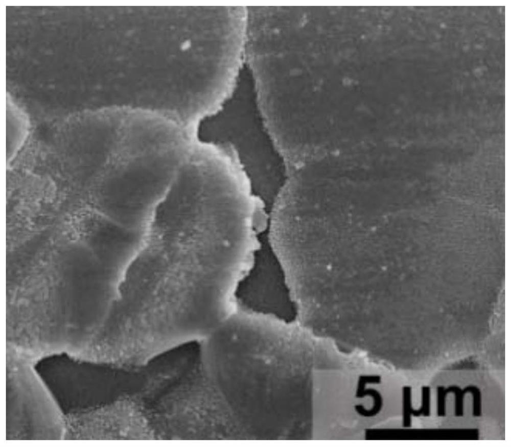
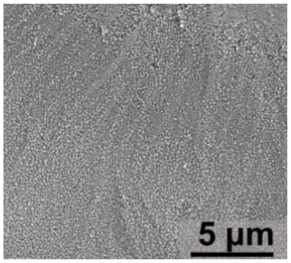
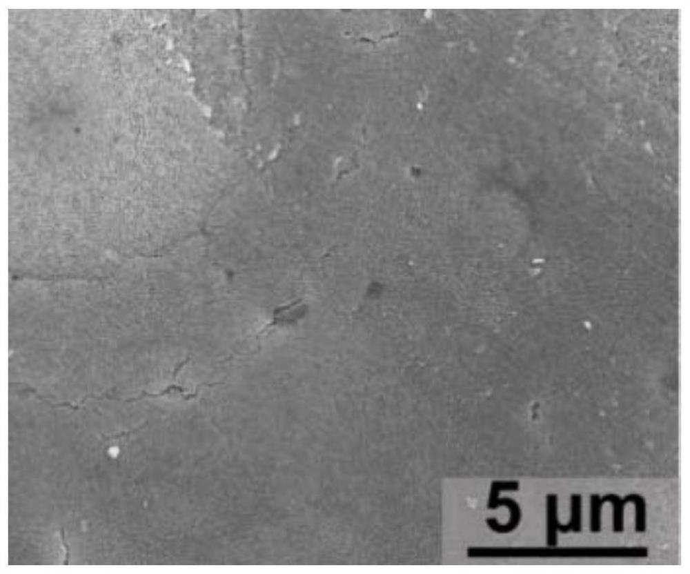
[0059] Embodiment 1: the preparation of perovskite film, photodetector
[0060] A kind of anti-solvent preparation method of perovskite film, comprises the following steps:
[0061] Preparation of perovskite precursor solution: In a nitrogen glove box environment, add 0.4mmol of phenethylamine iodine salt (PEAI) particle powder and 0.2mmol of PbI successively in a glass bottle 2 powder, then add 4mL dimethylformamide (DMF) and let it stand for more than 1h to obtain the perovskite precursor solution;
[0062] SiO with a size of 2.5cm×2.5cm 2 The glass substrate is first cleaned with detergent to clean the oil film on the glass surface, then completely cleaned with deionized water, then ultrasonicated with ethanol for 10 minutes, and finally placed in a plasma cleaning device for modification treatment for 5 minutes to obtain Modified substrate; the working conditions of the plasma cleaning equipment are: the working current is not greater than 1.2A, the power of the RF power...
Embodiment 2
[0067] Embodiment 2: the preparation of perovskite film, photodetector
[0068] Compared with Example 1, the only difference of Example 2 is that in Example 2, the temperature of the hot stage is increased to 100° C. for 5 minutes of annealing. The photodetector prepared in this embodiment was tested under the test conditions that the test wavelength was 475nm, and the optical power of the light source was constant at 14.5W / m 2 , the test area is 1.2mm 2 , the results show that the photodetector has a responsivity of 642μA / W, an external quantum efficiency of 0.17, and a specific detectivity of 3.52×10 8 Jones.
Embodiment 3
[0069] Embodiment 3: the preparation of perovskite film, photodetector
[0070] Compared with Example 1, the only difference of Example 3 is that in Example 3, the temperature of the hot stage was increased to 120° C. for 5 minutes of annealing. The photodetector prepared in this embodiment was tested under the test conditions that the test wavelength was 475nm, and the optical power of the light source was constant at 14.5W / m 2 , the test area is 1.2mm 2 , the results show that the photodetector has a responsivity of 669μA / W, an external quantum efficiency of 0.17, and a specific detectivity of 2.79×10 8 Jones.
PUM
| Property | Measurement | Unit |
|---|---|---|
| External quantum efficiency | aaaaa | aaaaa |
| External quantum efficiency | aaaaa | aaaaa |
Abstract
Description
Claims
Application Information


