Thin film type semiconductor chip structure and photoelectric device using same

A chip structure and semiconductor technology, applied in the direction of semiconductor devices, semiconductor lasers, optical waveguide semiconductor structures, etc., can solve the problems of current congestion, quantum efficiency, unresolved and insufficient sidewall light escape, and achieve suppression of non-radiative recombination heating , Improve light extraction efficiency and low device internal resistance

Pending Publication Date: 2021-12-28
DR TECH CO LTD YIXING JIANGSU
View PDF15 Cites 1 Cited by
  • Summary
  • Abstract
  • Description
  • Claims
  • Application Information

AI Technical Summary

Problems solved by technology

[0006] In Patent Document 2, an N-type GaN layer, a light-emitting layer MQW, a P-type GaN layer, a transparent conductive film, a non-conductive high-reflection film, and conductive holes running through it are disclosed from top to bottom; N-type ohmic contact electrodes The column is filled with conductive holes, although the heat dissipation effect has been improved, but it is still insufficient; the problems of current congestion, quantum efficiency of electro-optical conversion, and side wall escape have not been solved.

Method used


Image

  • Thin film type semiconductor chip structure and photoelectric device using same
  • Thin film type semiconductor chip structure and photoelectric device using same
  • Thin film type semiconductor chip structure and photoelectric device using same

Examples


Embodiment 1

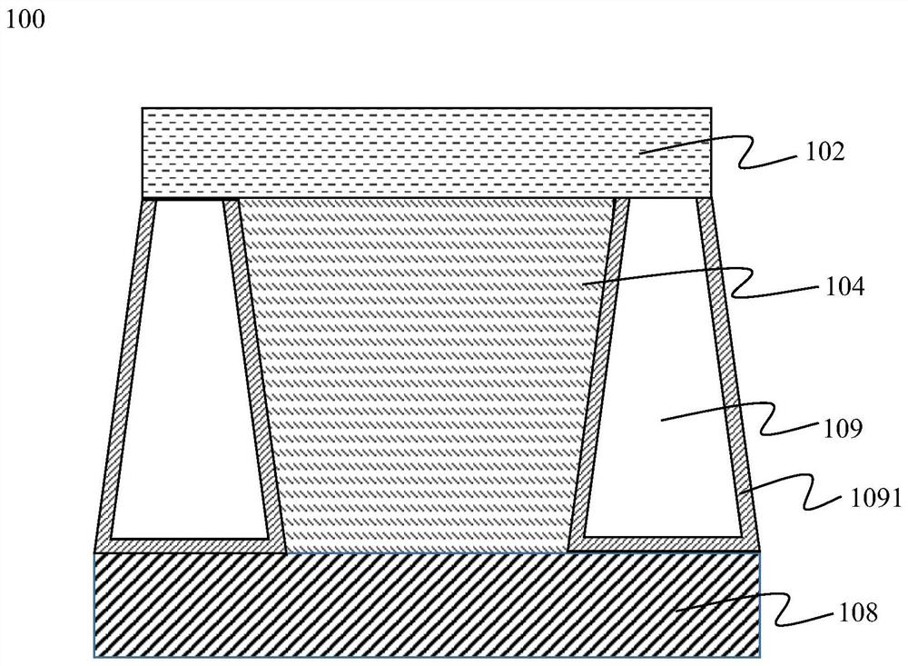
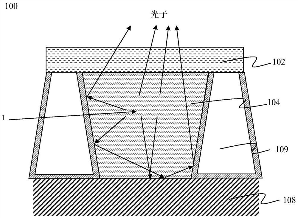
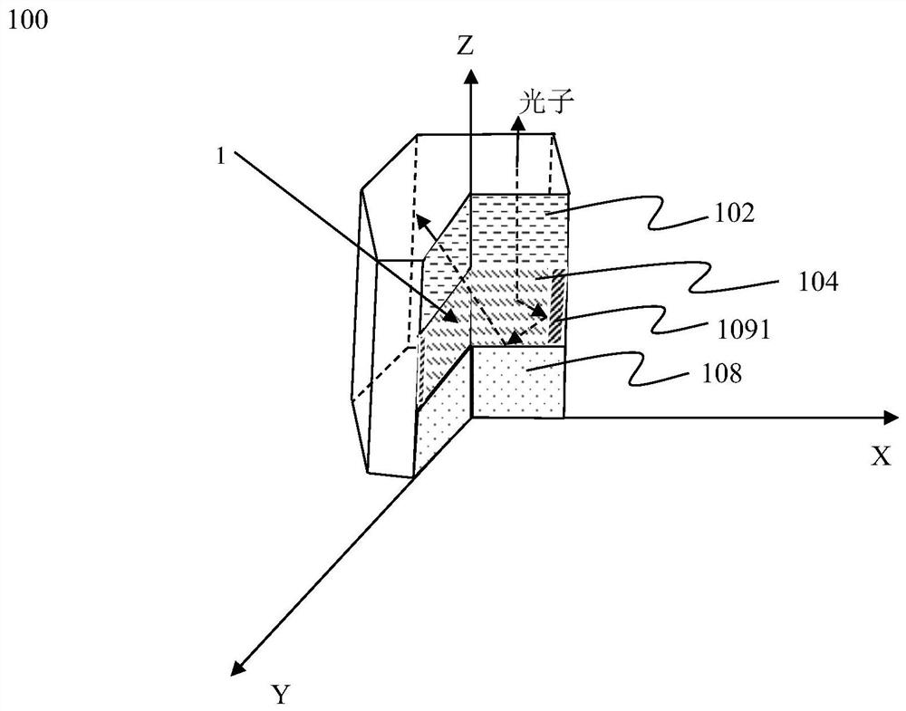
[0071] like figure 1 As shown, the thin film semiconductor chip structure according to Embodiment 1 of the present invention may be composed of one or more optical lattices 100 . The optical grid 100 includes a metal substrate 108 and a metal side wall 109 used as an electrode, and the metal substrate 108 and the metal side wall 109 are insulated and connected to each other to form an optical reflection cavity 1 (such as Figure 2A and 2B shown); the top of the optical reflective cavity 1 is covered with the first transparent conductive layer 102, and the first transparent conductive layer 102 is electrically connected with the metal sidewall 109, so that the optical grid 100 forms a closed structure. like Figure 2A and Figure 2B As shown, under the reflection of the metal substrate 108 and the metal sidewall 109, the photons can only pass through the first transparent conductive layer 102 on the top of the optical cell to exit. Inside the optical lattice, a photoelectri...

Embodiment 2

[0079] According to the attached Image 6 Another embodiment of the present disclosure will be described in detail.

[0080] Embodiment 2 is another specific implementation based on Embodiment 1. The optical grid 200 uses an epitaxial thin film layer to further improve the conversion efficiency of converting electrical energy into light energy, and finally increase the light extraction rate. It should be noted that the thin film layer with an epitaxial structure refers to a thin film layer grown on a substrate using an epitaxial process.

[0081] like Image 6 As shown, the photoelectric conversion layer adopts the multi-quantum well light-emitting layer 204 that converts electrical energy into light energy, and forms an electrical connection in series between the first transparent conductive layer 202 and the metal substrate 208 from top to bottom: the first current The confinement layer 203, the multi-quantum well light-emitting layer 204, the second current confinement la...

Embodiment 3

[0090] According to the attached Figure 7 Another embodiment disclosed in the present invention will be described in detail.

[0091] Arranging a plurality of light grids in Embodiment 2 together constitutes a "light grid array", which can be in a honeycomb shape. The whole device is a honeycomb light-emitting structure formed by the aggregation of many optical grids 200. The size of the optical grids in the honeycomb structure can be controlled by photolithography precision; preferably, the size of the light-emitting surface of each optical grid ranges from 10 μm to 500 μm, which can Extremely low internal resistance of the device to achieve high efficiency of electrical injection; the honeycomb structure has a three-dimensional reflective structure, which only retains the light emitted from the surface of the device, and at the same time eliminates the shading effect of the metal electrodes on the surface, plus the anti-reflection of the multi-layer structure on the surface...


PUM

PropertyMeasurementUnit
thicknessaaaaaaaaaa
thicknessaaaaaaaaaa
thicknessaaaaaaaaaa

Abstract

The invention relates to a thin film type semiconductor chip structure. The structure is named as a light grid structure. According to the structure, metal materials are utilized, one of P-type metal and N-type metal is made to serve as a substrate, and the other metal serves as a metal side wall. The metal side wall is in insulated connection with the metal substrate to form a three-dimensional optical reflection cavity. The top of the optical reflection cavity is covered with a transparent conductive layer, and a photoelectric conversion layer is arranged in the optical reflection cavity, so that a light grid is formed. When the photoelectric conversion layer converts electric energy into light energy, the light grid become a light-emitting unit; and when the photoelectric conversion layer converts light energy into electric energy, the light grid becomes a generation unit of the electric energy. The three-dimensional light grid structure can only emit or collect photons through the plane where the transparent conducting layer of the optical reflection cavity is located. A plurality of light grids are gathered together to form a light grid array. The invention also relates to an optoelectronic device using the light lattice structure.

Description

technical field [0001] The invention relates to a thin-film semiconductor chip structure in the semiconductor field and an optoelectronic device using the same. Background technique [0002] Light-emitting diodes made of III-V, II-IV, III-nitride, and III-arsenic-phosphide semiconductor light-emitting materials are used as the main body of the fourth-generation light source (semiconductor solid-state lighting). It has many advantages such as energy saving, environmental protection, long life, small size, light weight, shock resistance, good safety (low voltage drive), short response time, cold light source, rich colors, wide application range, etc. It is widely used in LCD backlight lighting source , automotive lighting, indoor and outdoor general lighting, display screens, traffic lights, landscape lighting, micro projectors, plant lighting, medical lighting equipment (such as: blue light for the treatment of jaundice) and many other fields. [0003] There are four common ...

Claims


Application Information

Patent Timeline
Patent Type & Authority Applications(China)
IPC IPC(8): H01L33/06H01L31/0352H01L33/14H01L33/30H01L33/60H01S5/20H01S5/22
CPCH01L33/06H01L33/60H01L33/145H01L33/305H01S5/2205H01S5/2009H01L31/035236H01L31/035272
Inventor 王伟明陈亮
Owner DR TECH CO LTD YIXING JIANGSU
Why Eureka
Try Eureka