Preparation method of spatially staggered mixed material film and application thereof in achromatic superlens

A technology of spatial interleaving and material thin film, applied in the direction of lens, metal material coating process, microscope, etc., can solve the problem of difficulty in realizing the interlaced local deposition of two semiconductor materials at the same time, and achieve the improvement of spot quality and achromatic performance, high The effect of transmittance and efficient focusing

Pending Publication Date: 2022-01-07
TIANJIN MEDICAL UNIV
View PDF2 Cites 0 Cited by
  • Summary
  • Abstract
  • Description
  • Claims
  • Application Information

AI Technical Summary

Problems solved by technology

[0004] The purpose of the present invention is to solve the technical problem that the existing metasurface device processing method is difficult to realize the interlaced and localized deposition of two semiconductor materials at the same time, and to provide a method for preparing a spatially interlaced mixed semiconductor material film and its application in an achromatic superlens

Method used


Image

  • Preparation method of spatially staggered mixed material film and application thereof in achromatic superlens
  • Preparation method of spatially staggered mixed material film and application thereof in achromatic superlens
  • Preparation method of spatially staggered mixed material film and application thereof in achromatic superlens

Examples


preparation example Construction

[0027] The method for preparing an achromatic superlens based on multi-step deposition of spatially interlaced mixed material films provided by the present invention mainly includes the following steps:

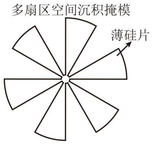
[0028] (1) Prepare a spatial deposition mask with a multi-sector structure: a thin silicon wafer with a thickness greater than the thickness of the thin film to be deposited (greater than 450 nm) is selected for the deposition mask. Under the microfabrication platform, using focused ion beam etching or femtosecond laser direct writing technology to process a multi-sector structure on a thin silicon wafer, its diameter is equivalent to the diameter of the expected metalens (between 40 μm and 100 μm). The spatial deposition mask is used for alternately covering subregions in the subsequent mixed material deposition process.

[0029] (2) Preparation of multi-step deposition of spatially interleaved mixed material films: first, the substrate is cleaned, and the substrate and mult...

Embodiment 1

[0037] Take the preparation of 920nm and 510nm dual-wavelength achromatic metalens and its application in two-photon fluorescence microscopy imaging as an example.

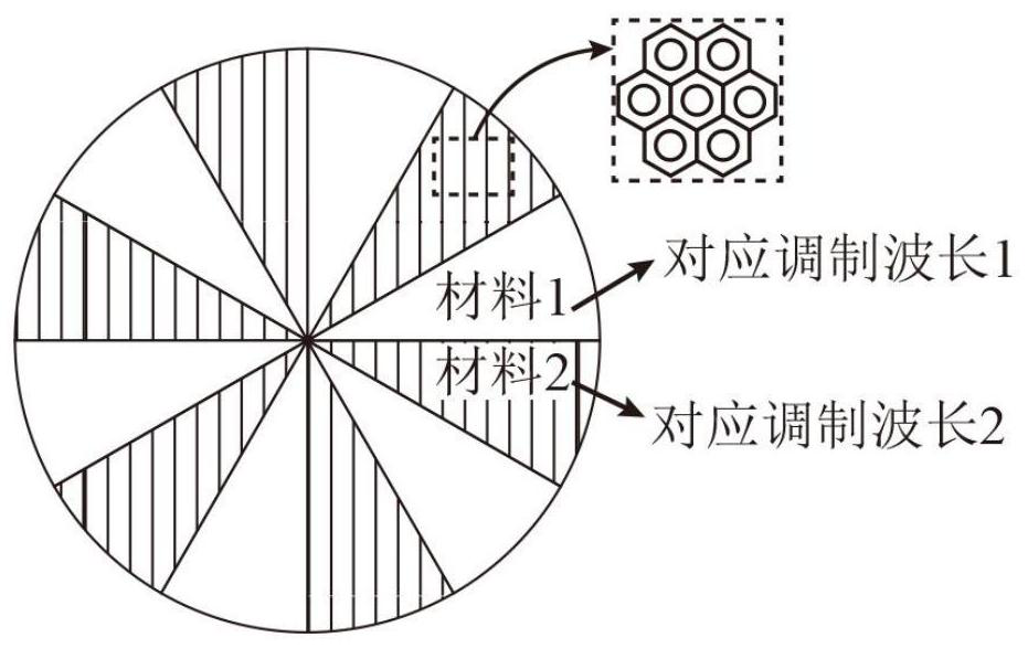
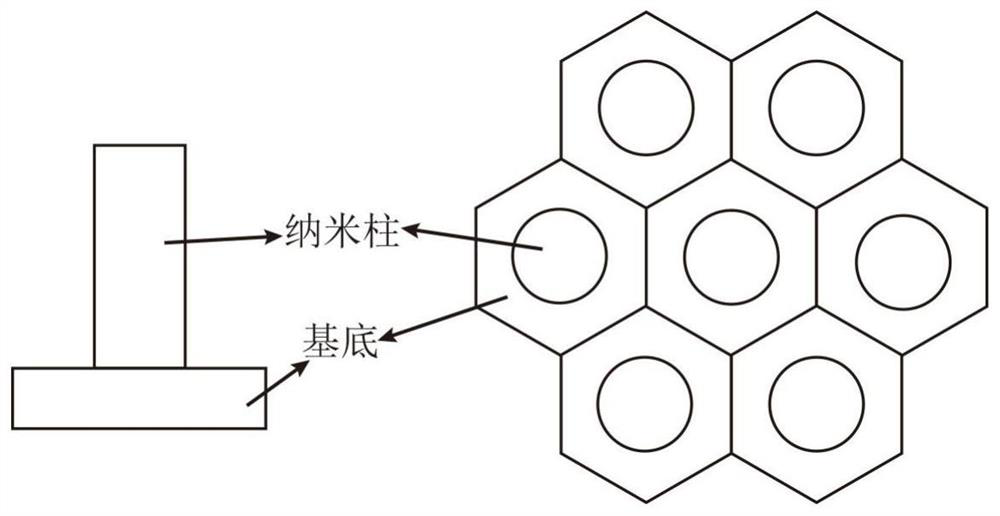
[0038] The planar structure diagram of the expected designed dual-wavelength achromatic metalens can be found in figure 1 , the superlens is composed of several nanopillars arranged in a regular hexagonal lattice structure. For the structure diagram of the nanounits, see figure 2 . Using green fluorescent protein as a fluorescent probe for two-photon fluorescence microscopy imaging, the two-photon excitation wavelength is 920nm, and the fluorescence wavelength is 510nm. Utilize above-mentioned processing method, at first process out multi-sector thin silicon chip (see specification attached image 3 ); and then deposit a dual-material thin film with a spatially partitioned structure on the substrate, wherein the first material is amorphous silicon for modulating 920nm excitation light, and the second material s...

Embodiment 2

[0041] Take the preparation of 910nm and 650nm dual-wavelength achromatic metalens and its application in two-photon STED micro-endoscopy imaging as an example.

[0042] The planar structure diagram of the expected designed dual-wavelength achromatic metalens can be found in figure 1 , the superlens is composed of several nanopillars arranged in a regular hexagonal lattice structure. For the structure diagram of the nanounits, see figure 2 . The two-photon excitation wavelength is 910nm, the loss wavelength is 650nm, and the fluorescence wavelength is close to the loss wavelength. Utilize above-mentioned processing method, at first process out multi-sector thin silicon chip (see specification attached image 3 ); and then deposit a space-partitioned dual-material mixed film on the substrate, wherein the first material is amorphous silicon for modulating 910nm excitation light, and the second material is titanium dioxide for modulating 650nm loss light. For the processing f...


PUM

PropertyMeasurementUnit
thicknessaaaaaaaaaa
diameteraaaaaaaaaa
diameteraaaaaaaaaa

Abstract

The invention relates to a preparation method of a spatially staggered mixed material film and an application thereof in an achromatic superlens. The method comprises the following steps that firstly, a multi-sector spatial deposition mask is processed by using a thin silicon wafer, partitioned covering is carried out by using the multi-sector mask, and a first dielectric material film is deposited on a super lens substrate; after the mask and redundant materials are removed through an etching technology, another multi-sector mask is replaced, and a second dielectric material film with the same thickness is deposited on the remaining sectors; and finally, a nano structure of the superlens is processed through micro-nano technologies such as electron beam lithography and the like. The invention provides a new thought for preparing the high-efficiency dual-wavelength achromatic superlens and applying the high-efficiency dual-wavelength achromatic superlens to two-photon microscopic imaging and two-photon STED super-resolution micro endoscopic imaging, the superlens realizes high-efficiency confocal of infrared band exciting light and visible band fluorescent light or loss light, therefore, the method is expected to be used in super-resolution micro endoscopic imaging of deep biological tissues of living bodies, and dynamic real-time super-resolution imaging with low invasion damage and high resolution is further realized.

Description

technical field [0001] The present invention relates to a method for preparing a thin film of a spatially interlaced mixed material in the field of dielectric metasurfaces and its application in an achromatic superlens, in particular to a method for preparing an achromatic superlens based on multi-step deposition of a thin film of a spatially interlaced mixed material, and the method The application of metalens in two-photon fluorescence microscopic imaging and two-photon stimulated emission depletion (Stimulated emission depletion, STED) super-resolution micro-endoscopic imaging belongs to the technical field of metasurface processing. Background technique [0002] As a miniature planar optical element, a metalens can flexibly manipulate the phase, polarization, and amplitude of light at the nanoscale. Due to its advantages of high degree of freedom and high integration, metalenses as miniature objective lenses have been applied in fluorescence microscopy imaging. In fluor...

Claims


Application Information

Patent Timeline
Patent Type & Authority Applications(China)
IPC IPC(8): C23C16/04C23C16/24C23C16/30C23C16/34C23C16/40C23C16/455C23C16/50C23C16/56G02B1/00G02B3/00G02B21/00G02B23/24
CPCC23C16/042C23C16/50C23C16/24C23C16/345C23C16/405C23C16/301C23C16/306C23C16/45525C23C16/56G02B1/002G02B3/00G02B21/0064G02B21/0072G02B23/2407G02B23/243
Inventor 刘淑静李阳赵世虎罗明艳巨丹丹
Owner TIANJIN MEDICAL UNIV
Why Eureka
Try Eureka