
Cu-high-entropy alloy thin film and preparation method thereof

A high-entropy alloy and thin-film technology, which is applied in metal material coating technology, ion implantation plating, coating, etc., can solve problems such as poor interface adhesion, increased resistance, and poor quality of pure copper oxides, and achieve thin-film Dense, well-bonded effect

Active Publication Date: 2022-01-11
XI AN JIAOTONG UNIV
View PDF6 Cites 3 Cited by
  • Summary
  • Abstract
  • Description
  • Claims
  • Application Information

AI Technical Summary

Problems solved by technology

However, the oxide quality of pure copper is poor, resulting in poor interfacial adhesion with the surrounding dielectric material, and cannot inhibit the migration of copper atoms into the dielectric material, easily causing short-circuit failures between components
Forming a Cu alloy by adding solid solution atoms to Cu can improve its bonding performance with the dielectric, and can increase the strength, but it will also increase the resistance

Method used


Image

  • Cu-high-entropy alloy thin film and preparation method thereof
  • Cu-high-entropy alloy thin film and preparation method thereof
  • Cu-high-entropy alloy thin film and preparation method thereof

Examples


Embodiment 1

[0029] Present embodiment 1 is implemented under the following implementation conditions and technical requirements:

[0030] Firstly, the monocrystalline silicon substrate was ultrasonically cleaned for 10 minutes each in analytical pure acetone and ethanol, and then quickly dried with warm air.

[0031] Immediately fix it on the substrate, mechanically and automatically send it into the magnetron sputtering vacuum coating chamber, and pump it until the vacuum degree of the background is 3.0×10 -4 Pa.

[0032] Then use magnetron sputtering dual DC power co-sputtering to deposit Cu-high entropy alloy thin film on the ultrasonically cleaned single crystal silicon wafer, wherein the Cu target purity is 99.99wt.%, using DC power supply, the power is 200W; high entropy TaNbHfZr The target purity is 99.95wt.%, and a DC power supply is used with a power of 20W. The deposition pressure was set at 0.3Pa, the deposition temperature was at room temperature, and the substrate rotation ...

Embodiment 2

[0036] This embodiment 2 is implemented under the following implementation conditions and technical requirements:

[0037] Firstly, the monocrystalline silicon substrate was ultrasonically cleaned for 10 minutes each in analytical pure acetone and ethanol, and then quickly dried with warm air.

[0038] Immediately fix it on the substrate, mechanically and automatically send it into the magnetron sputtering vacuum coating chamber, and pump it until the vacuum degree of the background is 3.0×10 -4 Pa.

[0039] Then use magnetron sputtering dual DC power co-sputtering to deposit Cu-high entropy alloy thin film on the ultrasonically cleaned single crystal silicon wafer, wherein the Cu target purity is 99.99wt.%, using DC power supply, the power is 200W; high entropy TaNbHfZr The target purity is 99.95wt.%, and a DC power supply is used with a power of 50W. The deposition pressure was set at 0.3Pa, the deposition temperature was at room temperature, and the substrate rotation spe...

Embodiment 3

[0043] This embodiment 3 is implemented under the following implementation conditions and technical requirements:

[0044] Firstly, the monocrystalline silicon substrate was ultrasonically cleaned for 10 minutes each in analytical pure acetone and ethanol, and then quickly dried with warm air.

[0045] Immediately fix it on the substrate, mechanically and automatically send it into the magnetron sputtering vacuum coating chamber, and pump it until the vacuum degree of the background is 3.0×10 -4 Pa.

[0046] Then use magnetron sputtering dual DC power co-sputtering to deposit Cu-high entropy alloy thin film on the ultrasonically cleaned single crystal silicon wafer, wherein the Cu target purity is 99.99wt.%, using DC power supply, the power is 200W; high entropy TaNbHfZr The target purity is 99.95wt.%, and a DC power supply is used with a power of 100W. The deposition pressure was set at 0.3Pa, the deposition temperature was at room temperature, and the substrate rotation sp...


PUM

PropertyMeasurementUnit
thicknessaaaaaaaaaa
hardnessaaaaaaaaaa
surface roughnessaaaaaaaaaa

Abstract

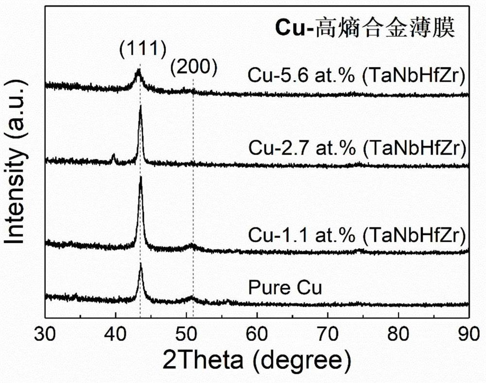
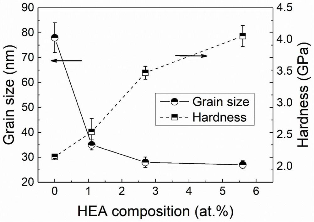
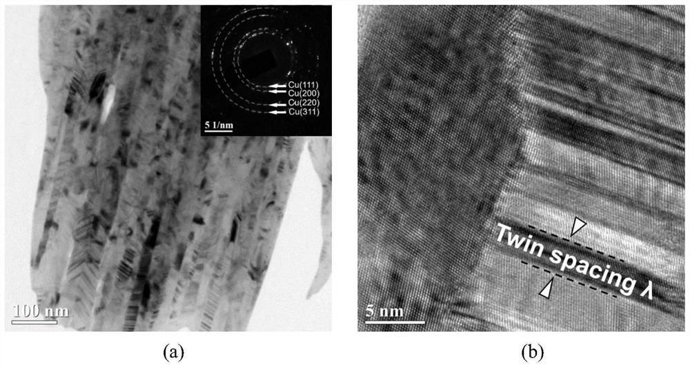
The invention discloses a Cu-high-entropy alloy thin film and a preparation method thereof. The Cu-high-entropy alloy thin film comprises the chemical component Cu-TaNbHfZr, wherein the atomic percent of the Cu-TaNbHfZr is as follows: copper is not less than 94.4, and the other element is a tantalum-niobium-hafnium-zirconium high-entropy alloy; the atomic percent of tantalum to niobium to hafnium to zirconium in the tantalum-niobium-hafnium-zirconium high-entropy alloy is 1: 1: 1: 1; a microstructure is complete nanocrystalline, and the grain size is 35.4 + / -2nm; the percentage of crystal grains containing nano-twin crystals is not lower than 90%, the thickness of the twin crystal lamellae is 2.4-3.5 nm, the advantages of the magnetron sputtering technology are utilized, the temperature in the deposition process is low, nanocrystal and nano-twin crystal structures can be formed easily, and alloy elements are macroscopically and evenly distributed through co-sputtering of different target materials, so that the multi-component alloying Cu thin film is obtained and is compact and well bonded with a matrix; the grain size is stabilized in the nano-crystal range, and a large number of nano-twin crystals are embedded in the grains; the alloy composition and components can be regulated and controlled; and the strength is high and the high thermal stability is good.

Description

technical field [0001] The invention belongs to the field of metal surface modification, and in particular relates to a Cu-high-entropy alloy thin film and a preparation method thereof. Background technique [0002] In MEMS, in order to further pursue advanced electronic devices with smaller size and lighter weight, it is a long-term task to develop Cu and Cu alloys with high strength and high thermal stability. However, the oxide quality of pure copper is poor, resulting in poor interfacial adhesion with the surrounding dielectric material, and cannot inhibit the migration of copper atoms into the dielectric material, easily leading to short-circuit failures between components. Adding solid-solution atoms to Cu to form a Cu alloy can improve its bonding performance with the dielectric, and can increase the strength, but it will also increase the resistance. In addition, the temperature rise of electronic devices will occur during electron transport, which also puts forward...

Claims


Application Information

Patent Timeline
Patent Type & Authority Applications(China)
IPC IPC(8): C23C14/18C23C14/34
CPCC23C14/185C23C14/3464
Inventor 张金钰李光亚王亚强吴凯刘刚孙军
Owner XI AN JIAOTONG UNIV
Learn More